Method and apparatus for processing substrates

a substrate and processing method technology, applied in the direction of electrical equipment, basic electric elements, electric discharge tubes, etc., can solve the problems of reducing the effective capacitance of the capacitor, affecting the processing efficiency of the capacitor, and affecting the processing efficiency of the substrate, so as to achieve the effect of improving the throughpu

Inactive Publication Date: 2007-03-22
KOKUSA ELECTRIC CO LTD
View PDF3 Cites 271 Cited by
  • Summary
  • Abstract
  • Description
  • Claims
  • Application Information

AI Technical Summary

Benefits of technology

[0011] It is, therefore, an object of the present invention to provide a substrate processing apparatus capable of uniformly removing a natural oxide film formed on each substrate to be processed without causing any plasma damage thereon but with an improved throughput.

Problems solved by technology

Thus, a film quality of the natural oxide film is inferior to that of a silicon oxide film formed through a controlled thermal oxidization process.
Accordingly, semiconductor devices manufactured by using the wafer having the natural oxide film formed thereon exhibit many an adverse effect on their device characteristics as follows.
1) The presence of a natural oxide film at the region of an insulation film of a capacitor on a wafer results in a reduced effective capacitance of the capacitor due to an increased distance between electrodes of the capacitor and also due to a low dielectric constant of the natural oxide film.
2) If a gate oxide film is formed on the natural oxide film, a leak current increases compared to a case without having a natural oxide film because the natural oxide film oxidized by oxygen in the ambient atmosphere contains a considerable amount of contaminants.
Further, since the contaminants contained in the natural oxide film may diffuse into neighboring layers thereof during a following heat-treatment process, electrical characteristics of a device can be deteriorated.
Further, since it is required to reduce a time between the finish of the cleaning processing and the beginning of the heat-treatment processing as to minimize the thickness of the natural oxide film which grows with time, a degree of design freedom of the processing line may be limited.
Still further, minute trenches of scaled-down semiconductor devices may not be properly cleaned through the HF cleaning process because the HF cleaning is a wet process.
However, the natural oxide film removing method through the use of the remote plasma cleaning technique has certain drawbacks as follows.
If a natural oxide film removing gas for dry-etching the natural oxide film is not properly activated, plasma damage may occur on the wafer or an etching selectivity may not be obtained, resulting in the failure to remove the natural oxide film.
Further, when a plurality of wafers are simultaneously processed so as to improve a throughput, if the uniformity of natural oxide film removing gas is not maintained between the wafers and within each wafer, the natural oxide films may not be removed uniformly.

Method used


Image

  • Method and apparatus for processing substrates
  • Method and apparatus for processing substrates
  • Method and apparatus for processing substrates

Examples


Embodiment Construction

[0030] Preferred embodiments of the present invention will now be described in detail with reference to the accompanying drawings.

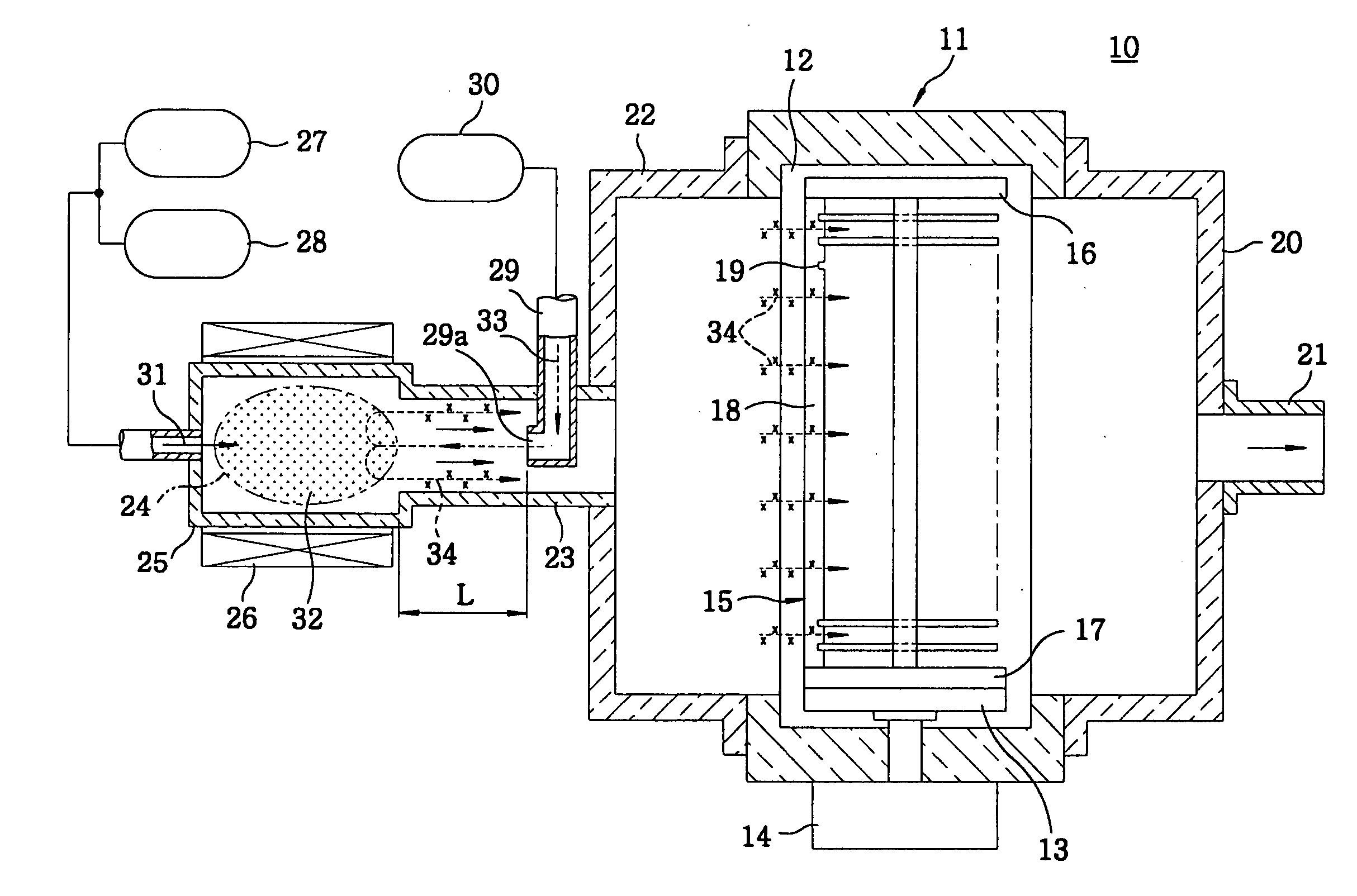
[0031] Referring to FIG. 1, there is illustrated a substrate processing apparatus in accordance with a first preferred embodiment of the present invention, which is a natural oxide films removing apparatus for removing a natural oxide film formed on a surface of a semiconductor wafer by using a remote plasma cleaning technique. As shown in FIG. 1, the natural oxide film removing apparatus 10 is configured to perform a batch process in which a plurality of the semiconductor wafers are simultaneously subject to a natural oxide film removing process.

[0032] As shown in FIG. 1, the natural oxide film removing apparatus 10 performing a batch process (hereinafter, referred to as a batch type natural oxide film removing apparatus) includes a process tube 11 forming therein a processing chamber 12 in which the natural oxide film removing process is carried out. ...


PUM

PropertyMeasurementUnit
angleaaaaaaaaaa
distanceaaaaaaaaaa
angleaaaaaaaaaa

Abstract

A substrate processing apparatus includes a processing chamber and a gas supply line, wherein a natural oxide film removing gas including a first gas activated by a second gas activated by a plasma discharge is supplied to the processing chamber through the gas supply line to remove a natural oxide film on a wafer, and wherein the first gas and the second gas are supplied to the gas supply line along a first direction and a second direction and an angle between the first and the second direction ranges from about 90° to 180°.

Description

FIELD OF THE INVENTION [0001] The present invention relates to a substrate processing apparatus; and, more particularly, to a method and apparatus for removing a natural oxide film formed on a substrate to be processed in the course of manufacturing, e.g., a semiconductor device. BACKGROUND OF THE INVENTION [0002] In manufacturing a semiconductor device, a batch type vertical hot wall furnace (hereinafter, referred to as a heat-treating apparatus) is widely used to perform a heat-treatment such as a film formation, an annealing process, an oxide film forming process or a diffusion process on silicon wafers (hereinafter, referred to as wafers). [0003] If a wafer is exposed to air while being transferred between processing stages of semiconductor device manufacturing processes, a natural oxide film is formed on the wafer due to oxygen or moisture in the air. The natural oxide film formed on the wafer is a silicon oxide film having an incomplete crystallinity. Thus, a film quality of t...

Claims


Application Information

Patent Timeline
Patent Type & Authority Applications(United States)
IPC IPC(8): H01L21/306H01L21/302H01J37/32H01L21/00H01L21/205H01L21/311
CPCH01J37/3244H01L21/67069H01L21/31116H01J2237/335
Inventor OGAWA, UNRYUTAKAGAKI, TETSUYAISHII, AKINORIUEDA, TATSUSHISATO, TAKAYUKI
Owner KOKUSA ELECTRIC CO LTD
Why Eureka
Try Eureka