

Nitride semiconductor device
a semiconductor and nitride technology, applied in semiconductor devices, semiconductor lasers, lasers, etc., can solve the problems of difficult to realize such expected effects of multiple quantum well structure active layers, difficult to achieve satisfactorily low ohmic contact as expected, and practicably such led devices or ld devices can be hardly fabricated, so as to achieve the effect of preferably improving the electrical resistance of the voltag
- Summary
- Abstract
- Description
- Claims
- Application Information
AI Technical Summary
Benefits of technology
Problems solved by technology
Method used
Image

Examples
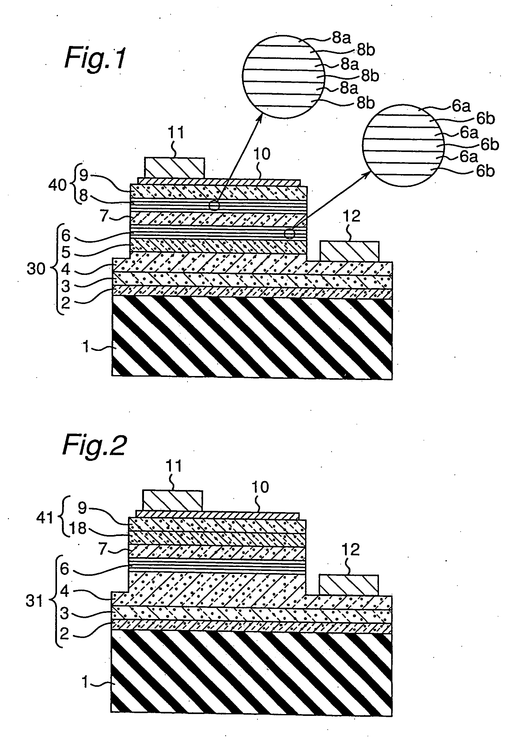
embodiment 1
Modification of Embodiment 1
[0139] Although in describing the first preferred embodiment of the present invention, reference has been made to the light emitting diode (LED) device, the present invention can be equally applied not only to the light emitting diode device, but also to a laser diode (LD) device which will now be described.
[0140] Specifically, in the LD device, the n-side multi-film layer, for example, is formed by alternately depositing one or more first nitride semiconductor films of InGaN and one or more second nitride semiconductor films of GaN with the or each first nitride semiconductor film having a different film thickness that progressively increases with decrease of the distance thereof to the active layer. With the n-side multi-film layer so constructed, that is to say, InGaN having a higher refraction index than that of GaN increases towards the active layer so that the n-side multi-film layer have a grading refraction index progressively increasing with dec...
embodiment 2
[0147] Hereinafter, the nitride semiconductor device according to a second preferred embodiment of the present invention will be described with reference to FIG. 4.
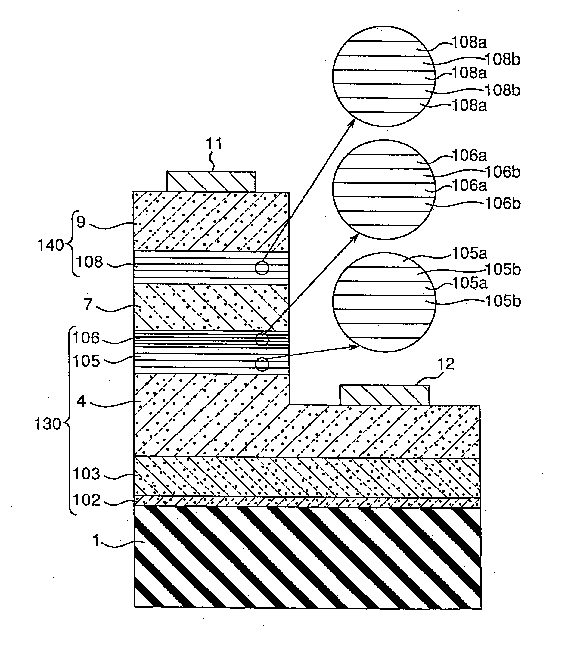
[0148] The nitride semiconductor device according to the second preferred embodiment of the present invention is a light emitting device of a double heterostructure comprising a substrate 1 having n-side and p-regions 130 and 140, each made up of a plurality of nitride semiconductor layers, with an active layer 7 of a multi quantum well structure intervening between the n- and p-regions 130 and 140.
[0149] More specifically, in the nitride semiconductor device according to the second embodiment, the n-region 130 comprises a sequentially laminated structure including, as shown in FIG. 4, a buffer layer 102 closest to the substrate surface, an undoped GaN layer 103, an n-contact layer 4 doped with n-type impurity, an n-side first multi-film layer 105 doped with n-type impurity, and a n-side second multi-film layer 106 remo...
embodiment 3
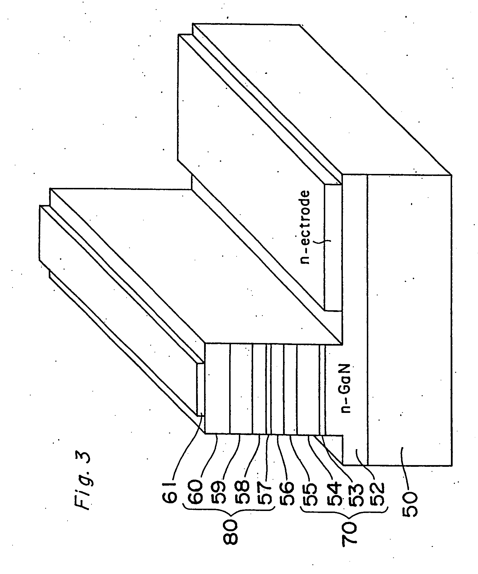
[0210] Now referring to FIG. 5, the embodiment 3 of the present invention will be described hereinafter.
[0211] As shown in FIG. 5, a nitride semiconductor light emitting device according to the third preferred embodiment of the present invention, comprises, on a substrate 1 of material such as sapphire via a buffer layer 202, an n-side first nitride semiconductor layer 203, an n-side second nitride semiconductor layer 204, an n-side third nitride semiconductor layer 205, an active layer 7, a p-cladding layer 108, and a p-contact layer 208 formed subsequently thereon. In this embodiment 3, a transparent p-electrode 10 is formed on the approximately entire top surface of the p-contact layer 208 and a p-pad electrode 11 for bonding is formed on a portion of the p-electrode 11. Also the emitting device has a portion where a surface of the n-side nitride semiconductor layer 204 is exposed and an n-electrode 12 is formed thereon.
[0212] As shown in FIG. 5, the nitride semiconductor light...
PUM
 Abstract
Description
Claims
Application Information