Epitaxially coated silicon wafer and method for producing epitaxially coated silicon wafers

a technology of epitaxial coating and silicon wafer, which is applied in the direction of polycrystalline material growth, chemically reactive gas growth, crystal growth process, etc., can solve the problems of uneven thickness of the inability to produce epitaxial coating silicon wafers with good global flatness, etc., to achieve the effect of improving global flatness and reducing hydrogen flow

Active Publication Date: 2007-03-22
SILTRONIC AG
View PDF20 Cites 33 Cited by
  • Summary
  • Abstract
  • Description
  • Claims
  • Application Information

AI Technical Summary

Benefits of technology

[0028] An object of the invention was to provide a method for epitaxially coating silicon wafers which makes it possible to provide epitaxially coated wafers having improved global flatness. These and other objects are achieved by a method for producing epitaxially coated silicon wafers, comprising providing a multiplicity of silicon wafers polished at least on their front sides, and successively and individually coating each wafer in an epitaxy reactor by a procedure in which a respective one of the silicon wafers is placed on a susceptor in the epitaxy reactor, is pretreated under a hydrogen atmosphere at a first hydrogen flow rate in a first step, and with addition of an etching medium to the hydrogen atmosphere at a reduced hydrogen flow rate in a second step, is subsequently coated epitaxially on its polished front side and is then removed from the epitaxy reactor, and furthermore an etching treatment of the susceptor is effected after a specific number of epitaxial coatings.

Problems solved by technology

However, the polishing of a silicon wafer usually gives rise to a decrease in the thickness of the planar silicon wafer toward the edge (“edge roll-off”).
Etching methods also tend to attack the silicon wafer to a greater extent at the edge, and therefore also produce such an edge roll-off.
The production of epitaxially coated silicon wafers with good global flatness proves to be extremely difficult since, as mentioned above, a concavely polished silicon wafer is usually present as the substrate.
However, such a non-uniform deposition is not considered in the epitaxy of silicon wafers since an important specification of an epitaxially coated silicon wafer, namely a limit value for a regularity of the epitaxial layer, will be exceeded.

Method used


Image

  • Epitaxially coated silicon wafer and method for producing epitaxially coated silicon wafers
  • Epitaxially coated silicon wafer and method for producing epitaxially coated silicon wafers
  • Epitaxially coated silicon wafer and method for producing epitaxially coated silicon wafers

Examples


example

[0056] An epitaxial layer was deposited on a silicon wafer having a diameter of 300 mm that had been polished by means of CMP on its front side, in accordance with the prior art. The silicon wafer was concavely polished, that is to say had a concave initial geometry and an edge roll-off. During pretreatment of this silicon wafer in the epitaxy reactor, first, a pretreatment in a hydrogen atmosphere was effected at an H2 flow rate of 50 slm.

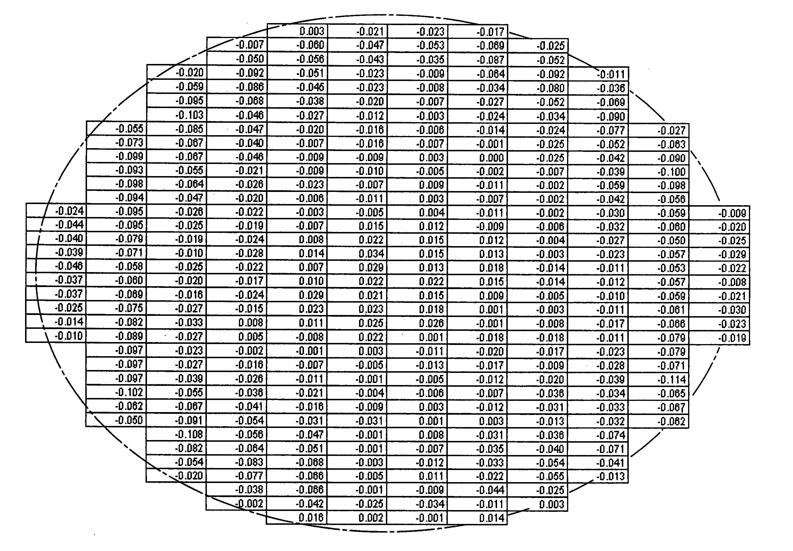
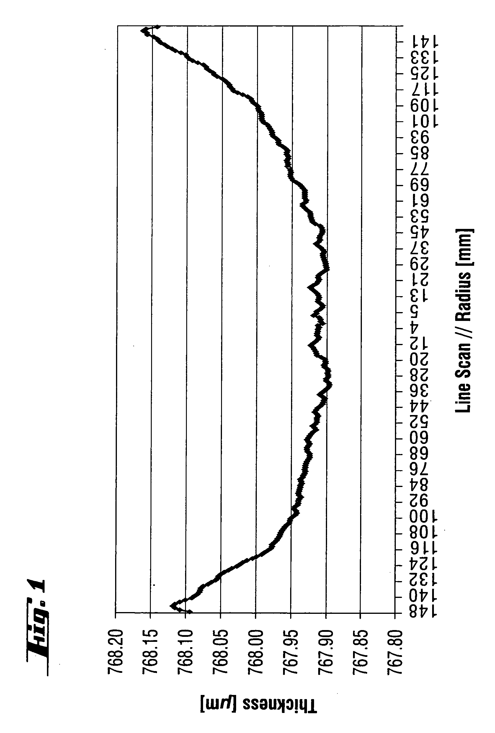
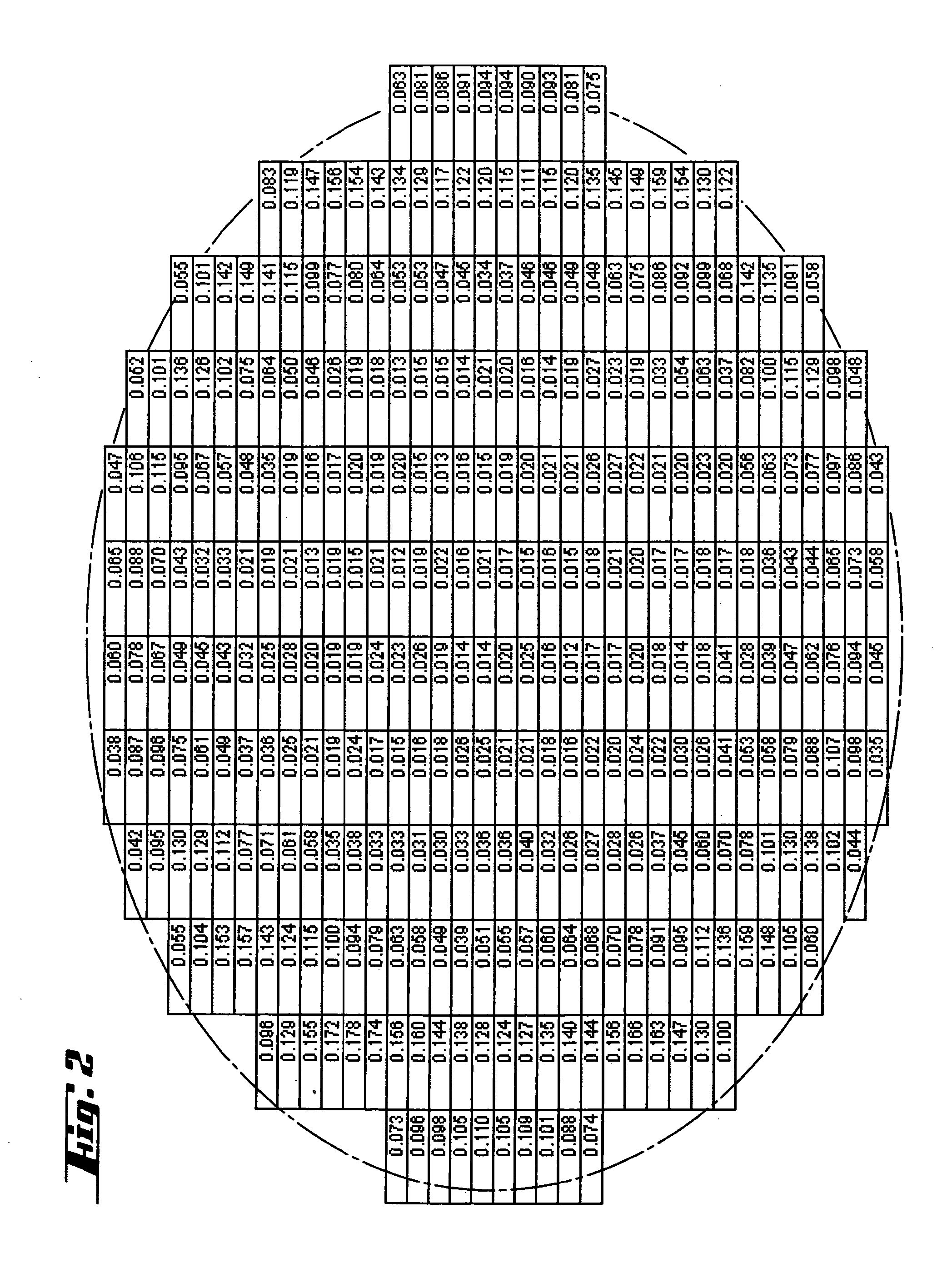
[0057] During a subsequent pretreatment, with hydrogen chloride added into the hydrogen atmosphere, the H2 flow rate was reduced according to the invention, to 5 slm. The duration of the pretreatment with hydrogen chloride was 60 s. An epitaxial layer was subsequently deposited at a deposition temperature of 1120° C. and a trichlorosilane flow rate of 17 slm. The results are explained below with reference to FIGS. 1 to 6, whereas FIGS. 2, 4 and 6 show schematically the geometry of the circular silicon wafers in perspective.

[0058]FIG. 1 illustrat...


PUM

PropertyMeasurementUnit
temperatureaaaaaaaaaa
flatnessaaaaaaaaaa
sizeaaaaaaaaaa

Abstract

A multiplicity of silicon wafers polished at least on their front sides are provided and successively coated individually in an epitaxy reactor by a procedure whereby one of the wafers is placed on a susceptor in the epitaxy reactor, is pretreated under a hydrogen atmosphere at a first hydrogen flow rate, and with addition of an etching medium to the hydrogen atmosphere at a reduced hydrogen flow rate in a second step, is subsequently coated epitaxially on its polished front side, and removed from the reactor. An etching treatment of the susceptor follows a specific number of epitaxial coatings. Silicon wafers produced thereby have a global flatness value GBIR of 0.07-0.3 μm relative to an edge exclusion of 2 mm.

Description

BACKGROUND OF THE INVENTION [0001] 1. Field of the Invention [0002] The invention relates to an epitaxially coated silicon wafer and to a method for producing epitaxially coated silicon wafers. [0003] 2. Background Art [0004] Epitaxially coated silicon wafers are suitable for use in the semiconductor industry, in particular for the fabrication of large scale integrated electronic components such as microprocessors or memory chips. Stringent requirements with respect to global and local flatness, thickness distribution, single-side-referenced local flatness (nanotopology) and freedom from defects are required of the starting materials (substrates) for modern microelectronics. [0005] Global flatness relates to the entire surface of a semiconductor wafer minus a defined edge exclusion. It is described by the GBIR, or “global backsurface-referenced ideal plane / range”, the magnitude of the positive and negative deviation from a backside-referenced ideal plane for the entire front side of...

Claims


Application Information

Patent Timeline
Patent Type & Authority Applications(United States)
IPC IPC(8): H01L21/20
CPCC30B25/02C30B29/06H01L21/02381H01L21/0243Y10S438/905H01L21/0262H01L21/02658H01L21/3065H01L21/02532H01L21/20
Inventor SCHAUER, REINHARDWERNER, NORBERT
Owner SILTRONIC AG
Why Eureka
Try Eureka