Method of manufacturing nitride semicondctor device

a technology of nitride and semiconductor, which is applied in the direction of semiconductor devices, basic electric elements, electrical apparatus, etc., can solve the problems of nitride semiconductor device electrical characteristics may be degraded, damage to the nitride semiconductor layer, and easy generation of heat by electrodes, so as to increase the absorption coefficient, prolong the absorption edge of the stripping layer, and reduce the effect of nitride semiconductor device damag

Inactive Publication Date: 2007-03-22
EPISTAR CORP
View PDF5 Cites 2 Cited by
  • Summary
  • Abstract
  • Description
  • Claims
  • Application Information

AI Technical Summary

Benefits of technology

[0013] Thereby, absorption coefficient of the stripping layer caused the decomposition is increased more than absorption coefficient of the nitride semiconductor layer and the substrate, and absorption edge of the stripping layer caused the decomposition is lengthened more than absorption edge of the nitride semiconductor layer and the substrate. That is, even if the composition of the stripping layer is close to the composition of the nitride semiconductor layer and the substrate, and the stripping layer is formed of thin film, it is possible to increase the absorption coefficient and lengthen the absorption edge of the stripping layer.
[0014] Therefore, as sufficiently minimizing the photon energy of the laser light irradiated to the stripping layer, compared to the band-gap energy of the nitride semiconductor layer and the substrate, the stripping layer absorbs the laser light. Accordingly, the nitride semiconductor can be easily separated from the substrate, and the degradation of the characteristics in the nitride semiconductor device caused by the laser light can be suppressed.
[0015] Moreover, even if the laser light irradiated to the stripping layer through the substrate, it is possible to suppress a generation of a crack and a decomposition of substrate caused from defects and impurity in the substrate. Also, even if the laser light reaches an electrode, affection of the laser light toward the electrode can be suppressed.

Problems solved by technology

That is, characteristics of the nitride semiconductor device (optical characteristics and electrical characteristics) may be degrade by the absorption of the laser light causing damages to the nitride semiconductor layer.
That is, the electrode easily generates heat and the electrical characteristics of the nitride semiconductor device may be degraded.

Method used


Image

  • Method of manufacturing nitride semicondctor device
  • Method of manufacturing nitride semicondctor device
  • Method of manufacturing nitride semicondctor device

Examples


first embodiment

(Method of Manufacturing a Nitride Semiconductor Device )

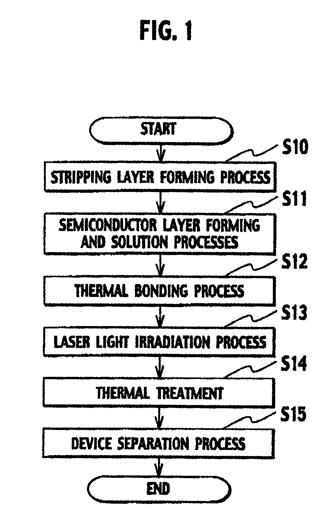
[0039] Hereinafter, descriptions will be provided for a method of manufacturing a light-emitting diode according to a first embodiment of the present invention with reference to FIGS. 1 to 7. FIG. 1 is a flowchart of the method of manufacturing a light-emitting diode according to a first embodiment of the present invention.

[0040] FIGS. 2 to 7 are cross-sectional views of the light-emitting diode according to the first embodiment in the course of manufacturing thereof.

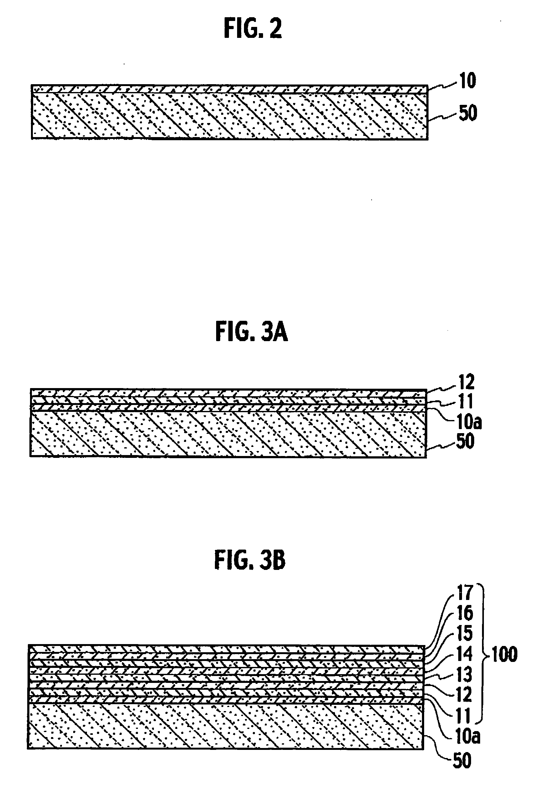
[0041] As shown in FIG. 1, a process of forming a stripping layer is performed in Step S10. At this point, as shown in FIG. 2, a stripping layer 10, which is formed of a nitride semiconductor containing In, is formed by use of an MOCVD (Metal Organic Chemical Vapor Deposition) method, on a growth substrate 50 formed of a GaN substrate.

[0042] Specifically, in a state where a growth substrate 50 is maintained at a growth temperature between about 700° C. and 1000...

second embodiment

(Method of Manufacturing a Nitride Semiconductor Device )

[0084] Hereinafter steps of a method of manufacturing a nitride semiconductor laser according to a second embodiment of the present invention will be further described respectively with reference to FIG. 1, and FIGS. 8 to 13.

[0085] Incidentally, differences between the second embodiment and the aforementioned first embodiment will be mainly described below.

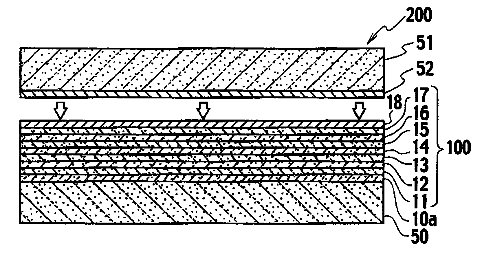
[0086] Specifically, in the first embodiment, the nitride semiconductor layer 100 is configured of the under layer 11, the n-type contact layer 12, the n-type cladding layer 13, the active layer 14, the p-type cap layer 15, the p-type cladding layer 16, and the p-type contact layer 17.

[0087] On the other hand, in the second embodiment, a nitride semiconductor layer 101 is configured of an under layer 21, an n-type contact layer 22, an n-type cladding layer 23, an n-type optical guiding layer 30, an active layer 24, a p-type cap layer 25, a p-type optical guiding layer 31,...

examples

[0113] Hereinafter, a comparison result of a relationship between a wavelength and an absorption ratio of the laser light irradiated to the stripping layer will be described, regarding the stripping layer before and after the decomposition caused. FIG. 14 shows the relationship between the wavelength and the absorption ratio of the stripping layer before and after the decomposition caused. Note that, horizontal axis shows the wavelength of the light and vertical axis shows absorption ratio of the light, in the FIG. 14.

[0114] As shown in FIG. 14, regarding the stripping layer before the decomposition caused, the wavelength band where the stripping layer absorbs the laser light sufficiently is short wavelength side only. For example, regarding the stripping layer before the decomposition caused, only the laser light of 400 nm or shorter can be used, to obtain the absorption ratio of 0.4 or more.

[0115] On the contrary, regarding the stripping layer after the decomposition caused, the...


PUM

PropertyMeasurementUnit
temperatureaaaaaaaaaa
thicknessaaaaaaaaaa

Abstract

A method of manufacturing a nitride semiconductor device includes the steps of, forming a stripping layer including In on a substrate; forming a nitride semiconductor layer on the stripping layer; causing a decomposition of the stripping layer by increasing a temperature of the stripping layer; irradiating the stripping layer with laser light; and separating the nitride semiconductor layer from the substrate.

Description

CROSS REFERENCE TO RELATED APPLICATIONS [0001] This application is based upon and claims the benefit of priority from prior Japanese Patent Application No. 2005-276854, filed on Sep. 22, 2005; and prior Japanese Patent Application No. 2006-249883, filed on Sep. 14, 2006; the entire contents of which are incorporated herein by reference. BACKGROUND OF THE INVENTION [0002] 1. Field of the Invention [0003] The present invention relates to a method of manufacturing a nitride semiconductor device. [0004] 2. Description of the Related Art [0005] In recent years, nitride semiconductor devices containing GaN, InN, AlN or the like, are heavily used as electronic device materials for blue and green light emitting diodes, light emitting devices such as blue-violet semiconductor lasers and high speed transistors operable at high temperatures. [0006] A manufacturing method is suggested, where a growth substrate is replaced with a metal substrate having high heat dissipation property after formin...

Claims


Application Information

Patent Timeline
Patent Type & Authority Applications(United States)
IPC IPC(8): H01L21/20H01L33/32
CPCH01L21/6835H01L21/76251H01L2221/68363H01L33/0095H01L2221/6835H01L33/0079H01L33/0093
Inventor KUNOH, YASUMITSUTAKEUCHI, KUNIO
Owner EPISTAR CORP
Why Eureka
Try Eureka