GaN crystal substrate, fabricating method of GaN crystal substrate, and light-emitting device

Active Publication Date: 2008-01-17
SUMITOMO ELECTRIC IND LTD
View PDF3 Cites 8 Cited by
  • Summary
  • Abstract
  • Description
  • Claims
  • Application Information

AI Technical Summary

Benefits of technology

[0018]According to the present invention, it is possible to provide a GaN crystal substrate having a small absorption coefficient of light, a fabrica

Problems solved by technology

In the case where a sapphire substrate is used as the substrate for a light-emitting device, it is not possible to form an electrode on a back surface of the sapphire substrate (opposite to the s

Method used


Image

  • GaN crystal substrate, fabricating method of GaN crystal substrate, and light-emitting device
  • GaN crystal substrate, fabricating method of GaN crystal substrate, and light-emitting device
  • GaN crystal substrate, fabricating method of GaN crystal substrate, and light-emitting device

Examples


Example

Example 1

[0051]1. Fabrication of GaN Crystal Substrate

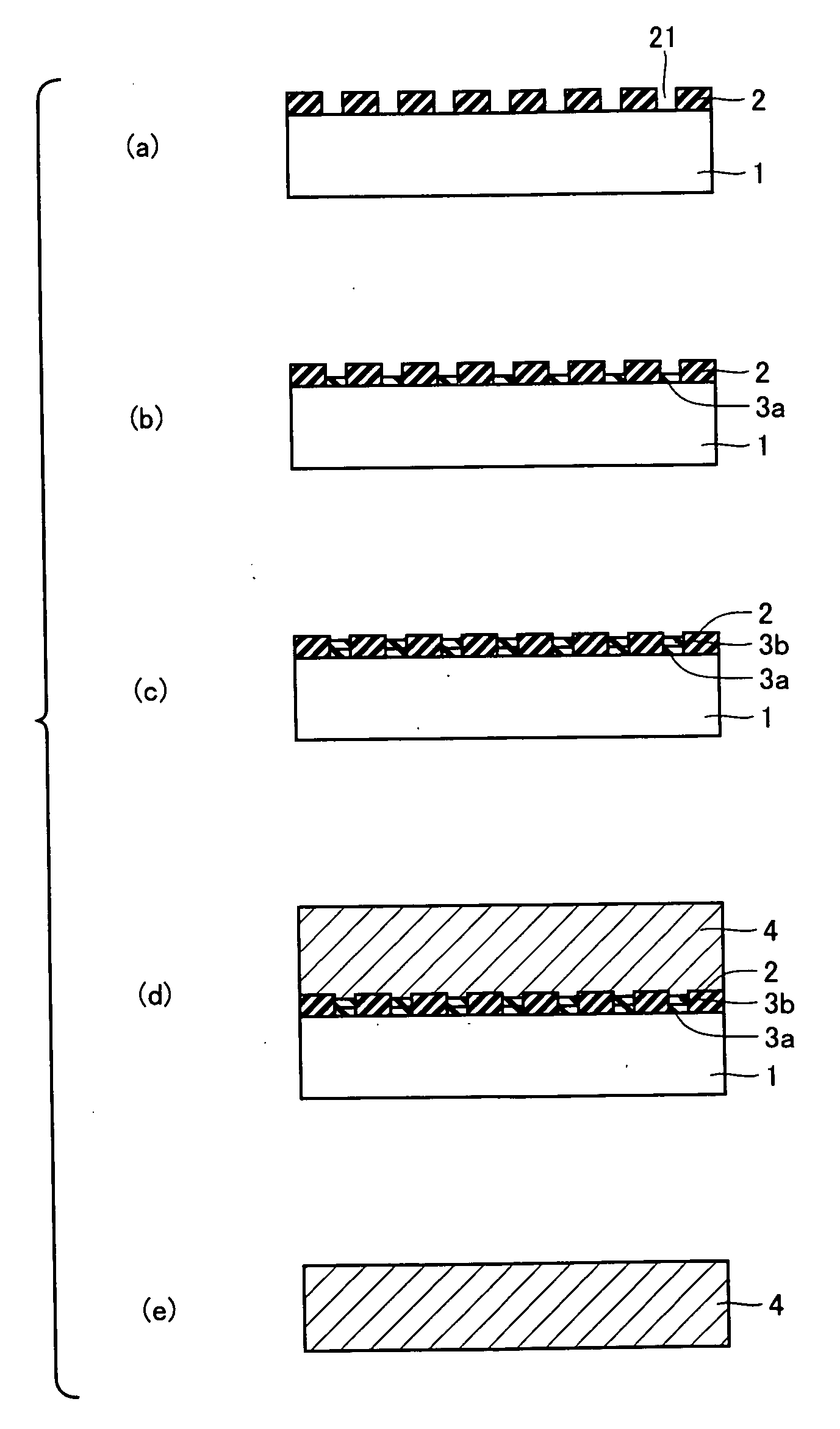
[0052]Firstly, on a GaAs substrate 1 having a diameter of 50 mm, a Si3N4 layer having a thickness of 100 nm was formed as a mask layer 2 by CVD under the atmospheric pressure, as shown in FIG. 1(a).

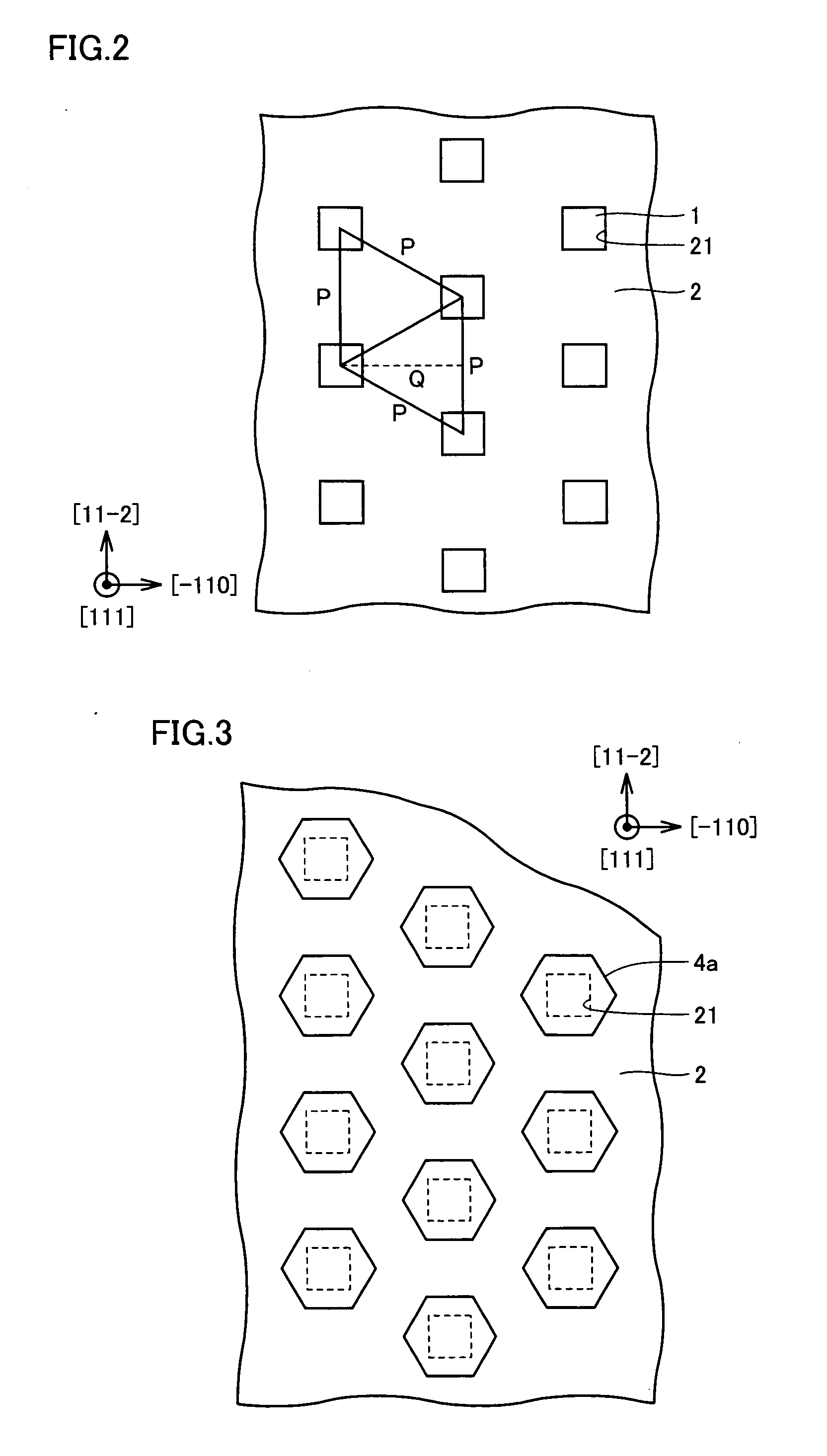
[0053]Thereafter, openings 21 were formed at mask layer 2 by photo etching to have centers corresponding to apexes of triangles with P of 4 μm and Q of 3.5 μm shown in FIG. 2. Here, opening 21 was shaped into a quadrate with a side of 1 μm.

[0054]Next, as shown in FIG. 1(b), a first GaN buffer layer 3a was grown to a thickness of 40 nm on the surface of GaAs substrate 1 exposed from openings 21 by HVPE, using HCl gas (partial pressure: 60.8 Pa) and NH3 gas (partial pressure: 1.31×10⁴ Pa) as the source gases, at the ambient temperature of 475° C.

[0055]Subsequently, as shown in FIG. 1(c), a second GaN buffer layer 3b was grown to a thickness of 40 nm on first GaN buffer layer 3a by HVPE, using HCl gas (partial pressure: 60.8 Pa) and NH3 g...

Example

Example 2

[0070]A GaN crystal substrate of Example 2 was fabricated in a similar manner and under similar conditions as in Example 1, except that mixed gas of O2 and N2 (partial pressure: 6.55×10² Pa) containing 0.1 mass % of O2 as well as HCl gas (partial pressure: 1.25×10³ Pa) and NH3 gas (partial pressure: 1.31×10⁴ Pa) were used as the source gases. The surface of the GaN crystal substrate of Example 2 had surface roughness Ra of 3 nm.

[0071]For the GaN crystal substrate of Example 2 thus obtained, the carrier concentration and the light absorption coefficient were evaluated in a similar manner and under similar conditions as in Example 1. The results are shown in Table 1.

[0072]As shown in Table 1, the GaN crystal substrate of Example 2 had the carrier concentration of 2×1019 cm−3, and the absorption coefficient of light of 375 nm wavelength was 68 cm−1, and the absorption coefficient of light of 500 nm wavelength was 10 cm−1. Since the light absorption coefficient becomes greater ...

Example

Example 3

[0075]A GaN crystal substrate of Example 3 was fabricated in a similar manner and under similar conditions as in Example 1, except that mixed gas of SiH4 and N2 (partial pressure: 93.5 Pa) containing 0.1 mass % of SiH4 as well as HCl gas (partial pressure: 1.25×10³ Pa) and NH3 gas (partial pressure: 1.31×10⁴ Pa) were used as the source gases. The surface of the GaN crystal substrate of Example 3 had surface roughness Ra of 3 nm.

[0076]For the GaN crystal substrate of Example 3 thus obtained, the carrier concentration and the light absorption coefficient were evaluated in a similar manner and under similar conditions as in Example 1. The results are shown in Table 1.

[0077]As shown in Table 1, the GaN crystal substrate of Example 3 had the carrier concentration of 5×1017 cm−3, and the absorption coefficient of light of 375 nm wavelength was 35 cm−1, and the absorption coefficient of light of 500 nm wavelength was 8 cm−1. Since the light absorption coefficient becomes greater a...


PUM


Abstract

A GaN crystal substrate is provided, which has a diameter of not less than 20 mm and a thickness of not less than 70 μm and not more than 450 μm, and has a light absorption coefficient of not less than 7 cm−1 and not more than 68 cm−1 for light in the wavelength range of not less than 375 nm and not more than 500 nm. A fabricating method of the GaN crystal substrate, and a light-emitting device fabricated using the GaN crystal substrate are also provided.

Description

BACKGROUND OF THE INVENTION[0001]1. Field of the Invention[0002]The present invention relates to a GaN (gallium nitride) crystal substrate, a fabricating method of the GaN crystal substrate, and a light-emitting device. More particularly, the present invention relates to a GaN crystal substrate having a small absorption coefficient of light, a fabricating method of the GaN crystal substrate, and a light-emitting device increased in optical output that is fabricated using the GaN crystal substrate.[0003]2. Description of the Background Art[0004]Currently, a sapphire substrate or a GaN crystal substrate is primarily used as a substrate for a light-emitting device such as a light-emitting diode (hereinafter, “LED”), a laser diode (hereinafter, “LD”) and the like.SUMMARY OF THE INVENTION[0005]In the case where a sapphire substrate is used as the substrate for a light-emitting device, it is not possible to form an electrode on a back surface of the sapphire substrate (opposite to the sur...

Claims


Application Information

Patent Timeline
IPC IPC(8): H01L31/0312
CPCC30B25/02H01L33/0075C30B29/406C30B25/04
Inventor MATSUOKA, TORUMOTOKI, KENSAKU
Owner SUMITOMO ELECTRIC IND LTD
Why Eureka
Try Eureka