Optical communication device provided with a reflector and method for forming a reflector in an optical communication device

Inactive Publication Date: 2007-03-29
FUJITSU LTD
View PDF11 Cites 224 Cited by
  • Summary
  • Abstract
  • Description
  • Claims
  • Application Information

AI Technical Summary

Benefits of technology

[0014] In an optical communication device having a construction such as described above, the transparent thin film layer, which is formed on one end surface of the optical medium by using a transparent material to which a metal that forms a chemical bond with gold (Au) is added, will be an underlying layer of the Au thin film layer. Since the transparent thin film layer is substantially transparent to the light that propagates through the optical medium, the transparent thin film layer does not function as a reflecting surface. Therefore, the Au thin film layer will be a reflecting surface that reflects the light coming from the end surface of the optical medium, so that little loss of light occurs at the reflector

Problems solved by technology

However, a reflector using Al raises a problem of causing loss of light because some absorption of light occurs in reflecting the light.
Also, a reflector using Ag has a drawback in that, since Ag is a material that is liable to be oxidized though little absorption occurs in reflecting the light, loss of light occurs due to decrease in the reflectivity according as the oxidation proceeds.
However, a reflector in which an Au thin film has been formed directly on an end surface of a waveguide chip raises a problem in that exfoliation of the Au thin film is liable to occur because the adhesion strength of the Au thin film to the waveguide chip is weak.
However, with the conventional technique that aims at improvement of the adhesion strength of an Au thin film by using a metal thin film such as Ti as an underlying layer, the light that is

Method used


Image

  • Optical communication device provided with a reflector and method for forming a reflector in an optical communication device
  • Optical communication device provided with a reflector and method for forming a reflector in an optical communication device
  • Optical communication device provided with a reflector and method for forming a reflector in an optical communication device

Examples


first embodiment

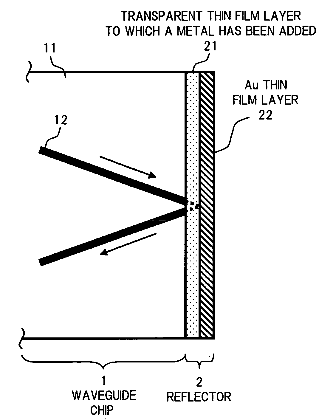
[0024]FIG. 1 is a plan view showing a construction of a principal part of an optical communication device according to the invention.

[0025] Referring to FIG. 1, the present optical communication device is provided, for example, with a waveguide chip 1 serving as an optical medium and a reflector 2 formed on one end surface of the waveguide chip 1.

[0026] The waveguide chip 1 has a waveguide 12 formed on an optical substrate 11. The scale reduction in the chip size is achieved by turning the waveguide 12 at the end surface of the optical substrate 11 in the same manner as in the above-described case shown in FIG. 6. As a material for the optical substrate 11, one can use, for example, lithium niobate (LiNbO3), silicon oxide (SiO2) used in a planar light-wave circuit (PLC), or a gallium arsenic (GaAs) based or indium phosphorus (InP) based optical semiconductor device, or the like.

[0027] The reflector 2 is made of a transparent thin film layer 21 and a gold (Au) thin film layer 22. W...

second embodiment

[0030] Next, the invention will be described.

[0031] In an optical communication device according to the second embodiment, a reflector 2 made of a transparent thin film layer 21 and an Au thin film layer 22 is formed on an end surface of a waveguide chip 1, in the same manner as in the construction of the above-described first embodiment shown in FIG. 1. The difference from the construction of the first embodiment lies in that the metal added to SiO2 as a material of the transparent thin film layer 21 is a metal that forms a complete solid solution with Au.

[0032] The metal that forms a complete solid solution with Au may be, for example, silver (Ag), platinum (Pt), or the like. At least one among these metals is added to SiO2. The kind and the concentration of the metal added to SiO2 are set by considering the effect for improvement of the adhesion strength of the Au thin film layer 22 and the transmittance of the transparent thin film layer 21, in the same manner as in the first e...

third embodiment

[0034] Next, the invention will be described.

[0035] In an optical communication device according to the third embodiment, a reflector 2 made of a transparent thin film layer 21 and an Au thin film layer 22 is formed on an end surface of a waveguide chip 1, in the same manner as in the construction of the above-described first embodiment shown in FIG. 1. The difference from the construction of the first embodiment lies in that the metal added to SiO2 as a material of the transparent thin film layer 21 is a metal having an oxide formation free energy of −6.3×10⁵ joule (=−150 kcal) or below.

[0036] The oxide formation free energy represents the reactivity of a metal to oxygen. A metal having a smaller value thereof, i.e. a metal that is more liable to be oxidized, has a stronger interfacial bond. Considering the interfacial bond with the Au thin film layer 22, when a metal having an oxide formation free energy of −6.3×10⁵ joule or below is contained in the transparent thin film layer 2...


PUM


Abstract

An optical communication device of the invention includes a reflector for reflecting the light that has reached one end surface of a waveguide chip to turn the optical path of the light. The reflector includes a transparent thin film layer formed on one end surface of the waveguide chip by using a material to which a metal that forms an intermetallic compound or the like with Au is added to a substance that is transparent to the light that propagates through the waveguide, as well as an Au thin film layer formed on the front surface of the transparent thin film layer. This allows formation of a reflector having an Au thin film layer as a reflecting surface in an optical medium with high adhesion strength. Thus, an optical communication device can be provided having a high reliability with little loss.

Description

BACKGROUND OF THE INVENTION [0001] (1) Field of the Invention [0002] The present invention relates to an optical communication device provided with a reflector for reflecting the light that has reached an end surface of an optical medium to turn the optical path thereof, and a method of forming a reflector in an optical communication device. Particularly, the invention relates to a technique for forming a reflector having a gold (Au) thin film as a reflecting surface with high adhesion strength. [0003] (2) Related Art [0004] In recent years, techniques using light are widely used. Among these, a communication technique using light is rapidly developing. Though a further multiple functionality, multiple-stage connection of plural functional sections, and the like are essential in devices used in the field of optical communication, there is also a high demand on a technique for scale reduction of devices. [0005] As one of the conventional techniques related to scale reduction of optic...

Claims


Application Information

Patent Timeline
IPC IPC(8): G02F1/33G02F1/01G02B26/08G02F1/295
CPCG02B5/08G02B2006/12119G02F1/116G02F2203/023G02F2201/16G02F2201/34G02F1/125
Inventor TSUNODA, YUKITOMIYATA, HIROSHI
Owner FUJITSU LTD
Why Eureka
Try Eureka