

Vertical cavity surface emitting semiconductor laser, light emission device, and optical transmission system
- Summary
- Abstract
- Description
- Claims
- Application Information
AI Technical Summary
Benefits of technology
Problems solved by technology
Method used
Image

Examples
example 1
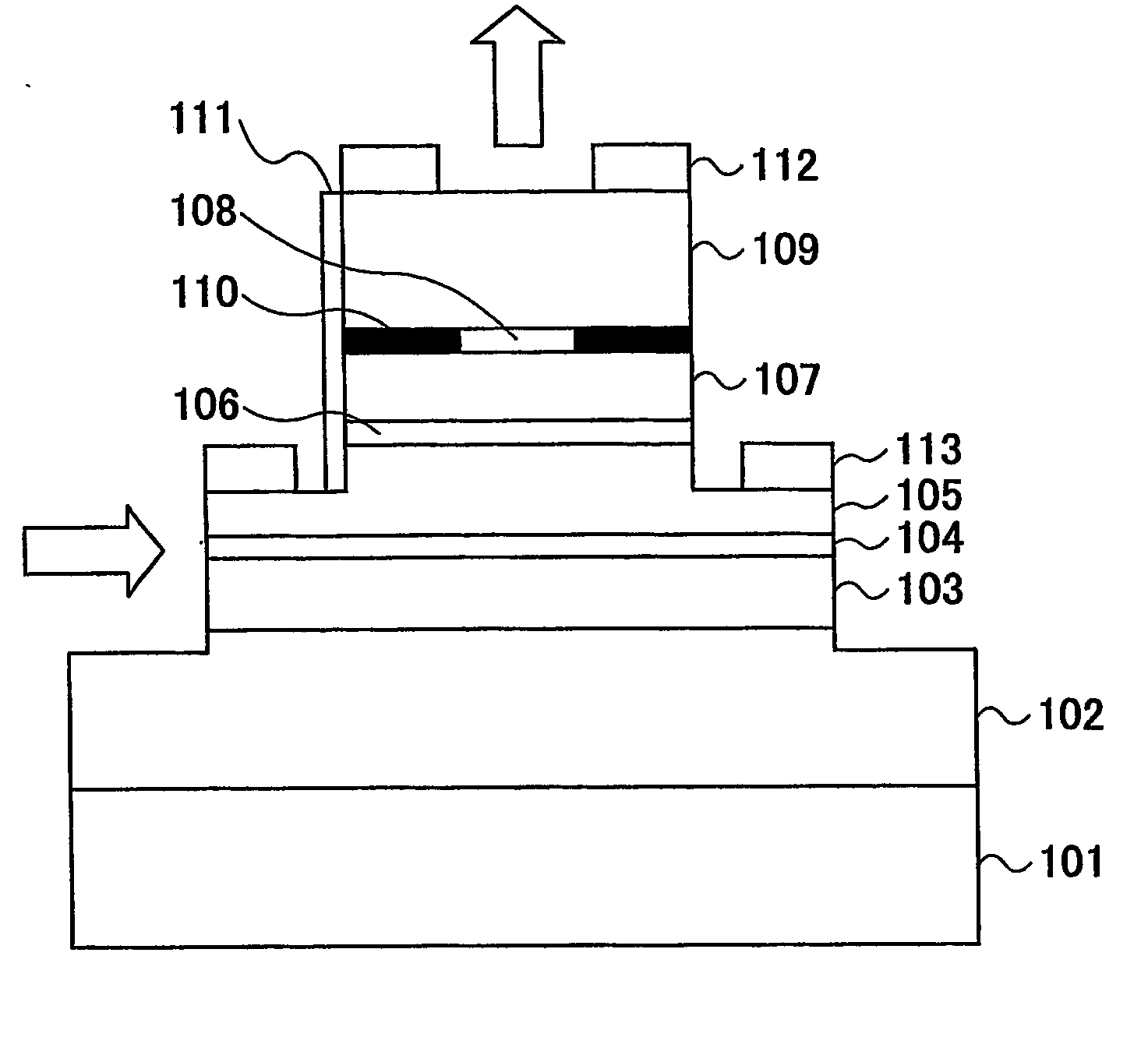
[0115]FIG. 1 is a schematic cross-sectional view illustrating an example of the vertical cavity surface emitting semiconductor laser (VCSEL) according to the present invention.
[0116] As illustrated in FIG. 1, a non-doped distributed Bragg reflection mirror (DBR) 102 is disposed on a semi-insulating GaAs substrate 101.
[0117] The non-doped distributed Bragg reflection. mirror (DBR) 102 is formed by alternately stacking a non-doped Al0.2Ga0.8As layer and a non-doped Al0.9Ga0.1As layer, each of which has a thickness of ¼ wavelength.
[0118] In addition, a first spacer layer 103 formed from Al0.3Ga0.7As, a multiple quantum well active region 104 formed from GaAs / Al0.3Ga0.7As, acting as the second active region, a second spacer layer 105 formed from n-type Al0.3Ga0.7As, a multiple quantum well active region 106 formed from GaAs / Al0.3Ga0.7As, acting as the first active region, a third spacer layer 107 formed from Al0.3Ga0.7As, a p-type AlAs layer 108, and a p-type DBR 109 are stacked sequ...
example 2
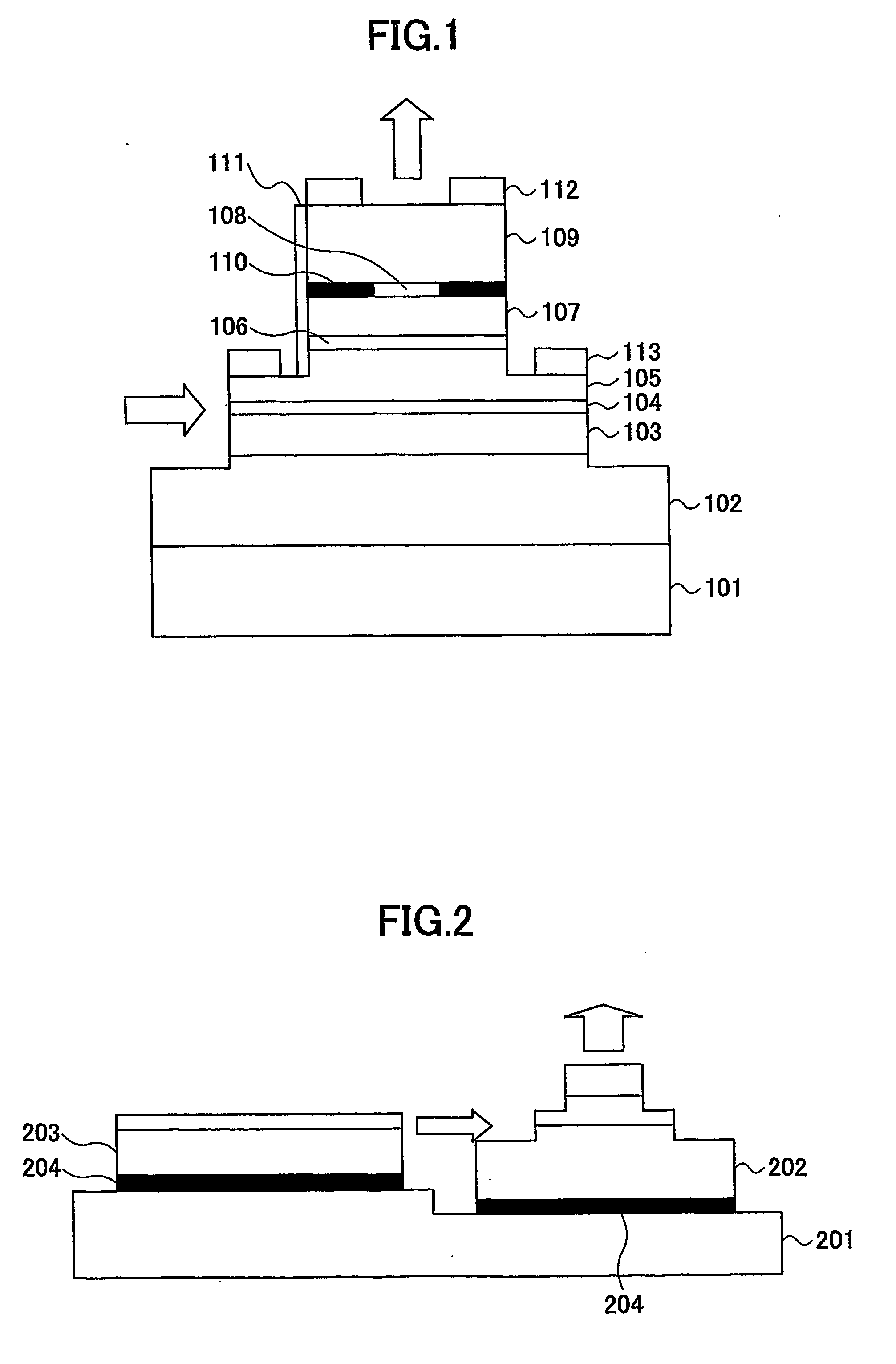
[0132]FIG. 2 is a schematic cross-sectional view illustrating an example of a light emission device, which includes the vertical cavity surface emitting semiconductor laser as shown in FIG. 1.
[0133] In this example, the same reference numbers are used for the same elements as those in the previous example, and overlapping descriptions being omitted.
[0134] As illustrated in FIG. 2, a VCSEL 202, as shown in FIG. 1, and an excitation semiconductor laser 203 are disposed on a silicon substrate 201. For example, the VCSEL 202 and the excitation semiconductor laser 203 are attached to the silicon substrate 201 by using a metal solder superior in thermal conductivity. For example, the excitation semiconductor laser 203 is a Fabry-Perot resonating semiconductor laser emitting a laser beam at a wavelength of 0.85 μm.
[0135] A step is formed on the silicon substrate 201 so that active layers of the excitation semiconductor laser 203 and the multiple quantum well second active region 104 for...
example 3
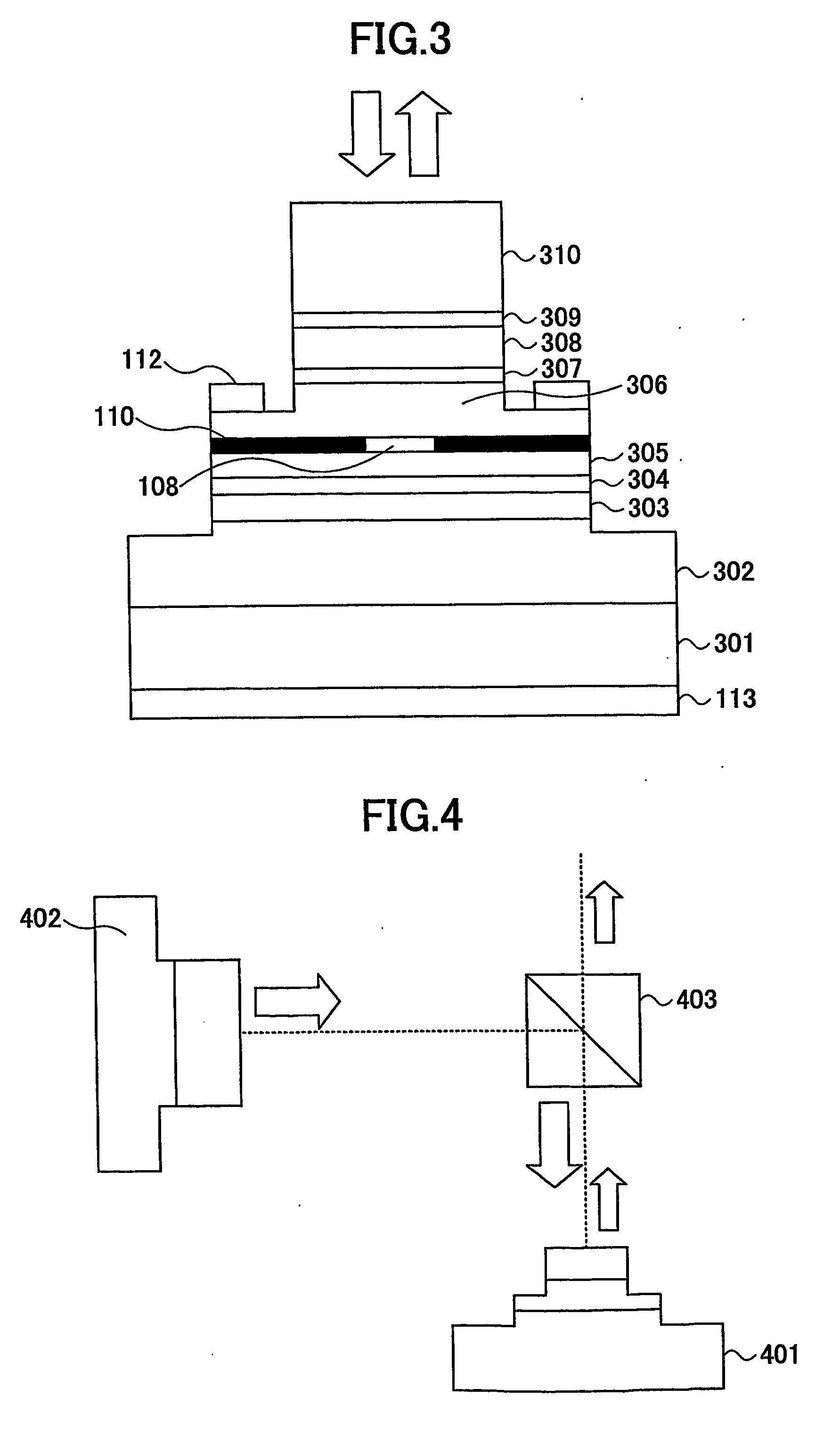
[0138]FIG. 3 is a schematic cross-sectional view illustrating another example of the vertical cavity surface emitting semiconductor laser (VCSEL) according to the present invention.
[0139] As illustrated in FIG. 3, an n-type distributed Bragg reflection mirror (DBR) 302 is disposed on an n-type GaAs substrate 301.
[0140] The n-type distributed Bragg reflection mirror (DBR) 302 is formed by alternately stacking an n-type GaAs layer and an n-type Al0.9Ga0.1As layer, each of which has a thickness of ¼ wavelength.
[0141] In addition, a first spacer layer 303 formed from GaAs, a multiple quantum well active region 304 formed from GaInNAs / GaAs, acting as the first active region, a second spacer layer 305 formed from GaAs, a p-type AlAs layer 108, a third spacer layer 306 formed from p-type GaAs, a multiple quantum well active region 307 formed from GaInNAs / GaAs, acting as the second active region, a fourth spacer layer 308 formed from GaAs, a multiple quantum well active region 309 formed...
PUM
 Abstract
Description
Claims
Application Information