[0012] In an illustrative embodiment an all-digital
readout integrated circuit (ROIC) in accordance with the principles of the present invention may be used in conjunction with a cryogenically cooled
infrared detector array, with connections between the
detector array and the ROIC made via
indium bump bonding. The
hybrid device thus formed is referred to herein as a digital focal plane array (DFPA). In an illustrative embodiment, the
detector array senses incoming
optical radiation in the
infrared region of the spectrum (2-20 microns) using photodiodes to create currents that are proportional to the
optical radiation impinging on the photodiodes. That is, each
photodiode (also referred to herein as a pixel) in the
detector array produces a current that is proportional to the
photon flux impinging upon it. Each
photodiode in the array has associated with it a unit
cell in the ROIC. The current in each
photodiode is collected in the photodiode's associated unit
cell within the ROIC. The unit
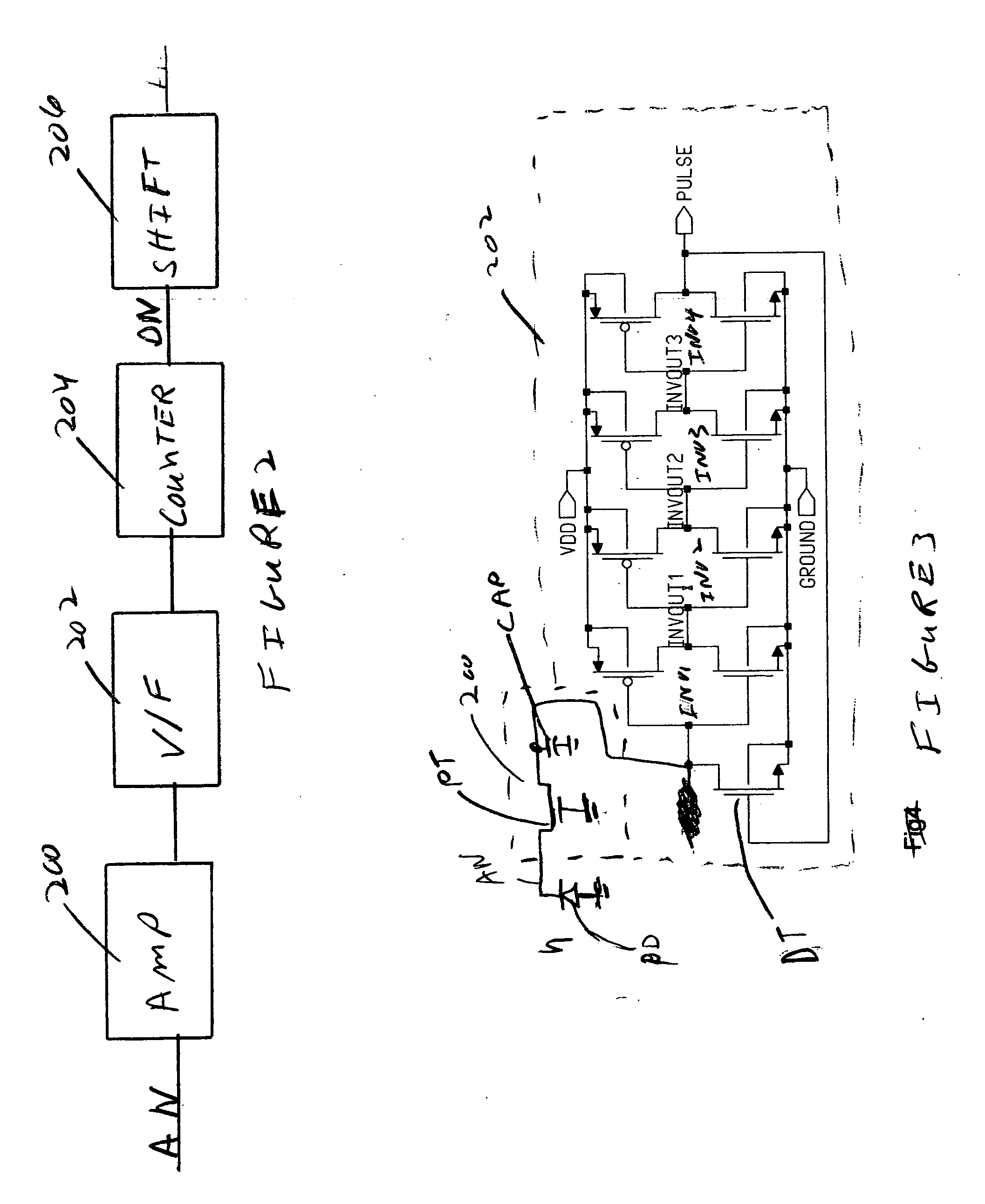
cell electronics integrate the charge and produces, via an
analog to digital converter (ADC), a
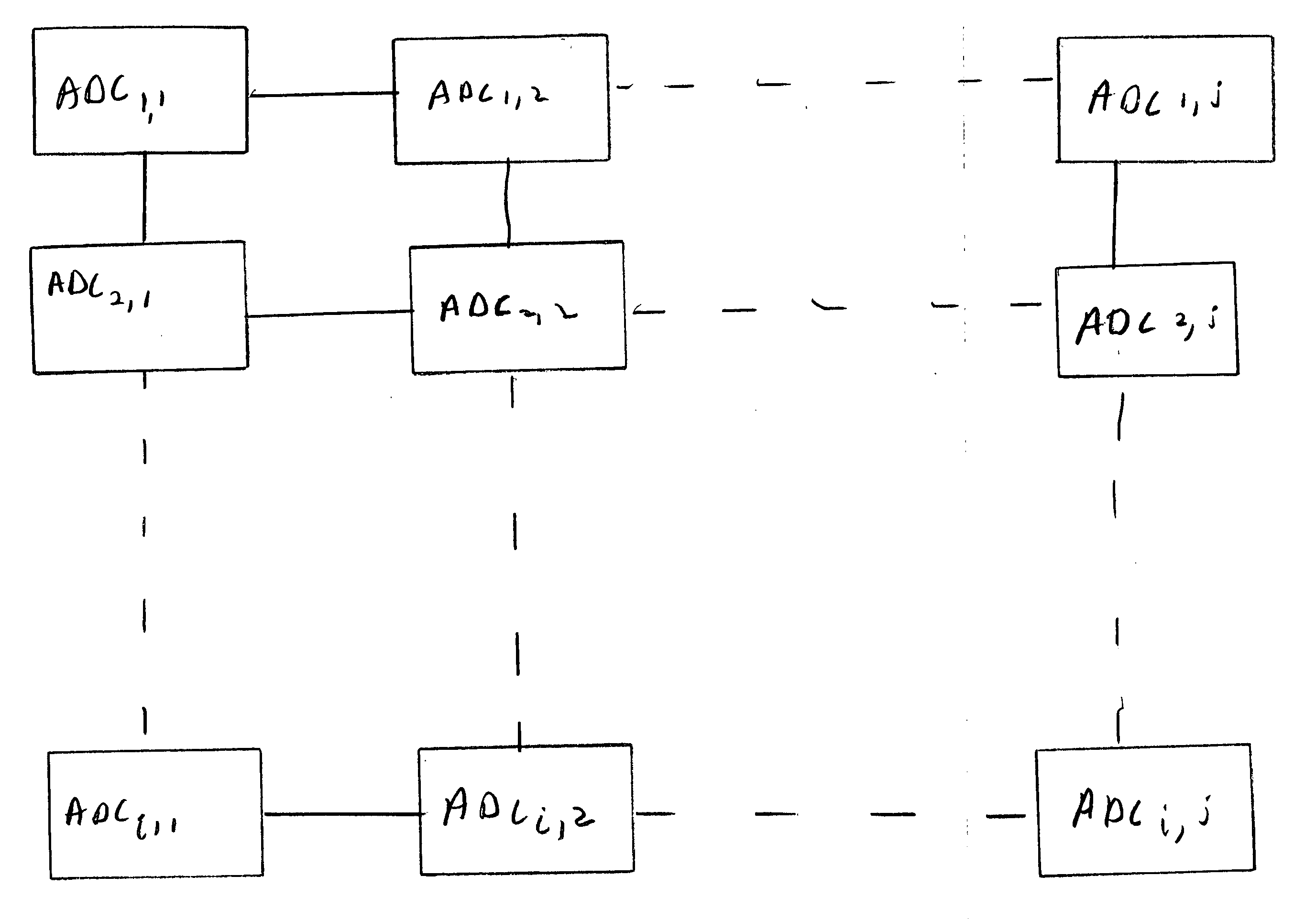
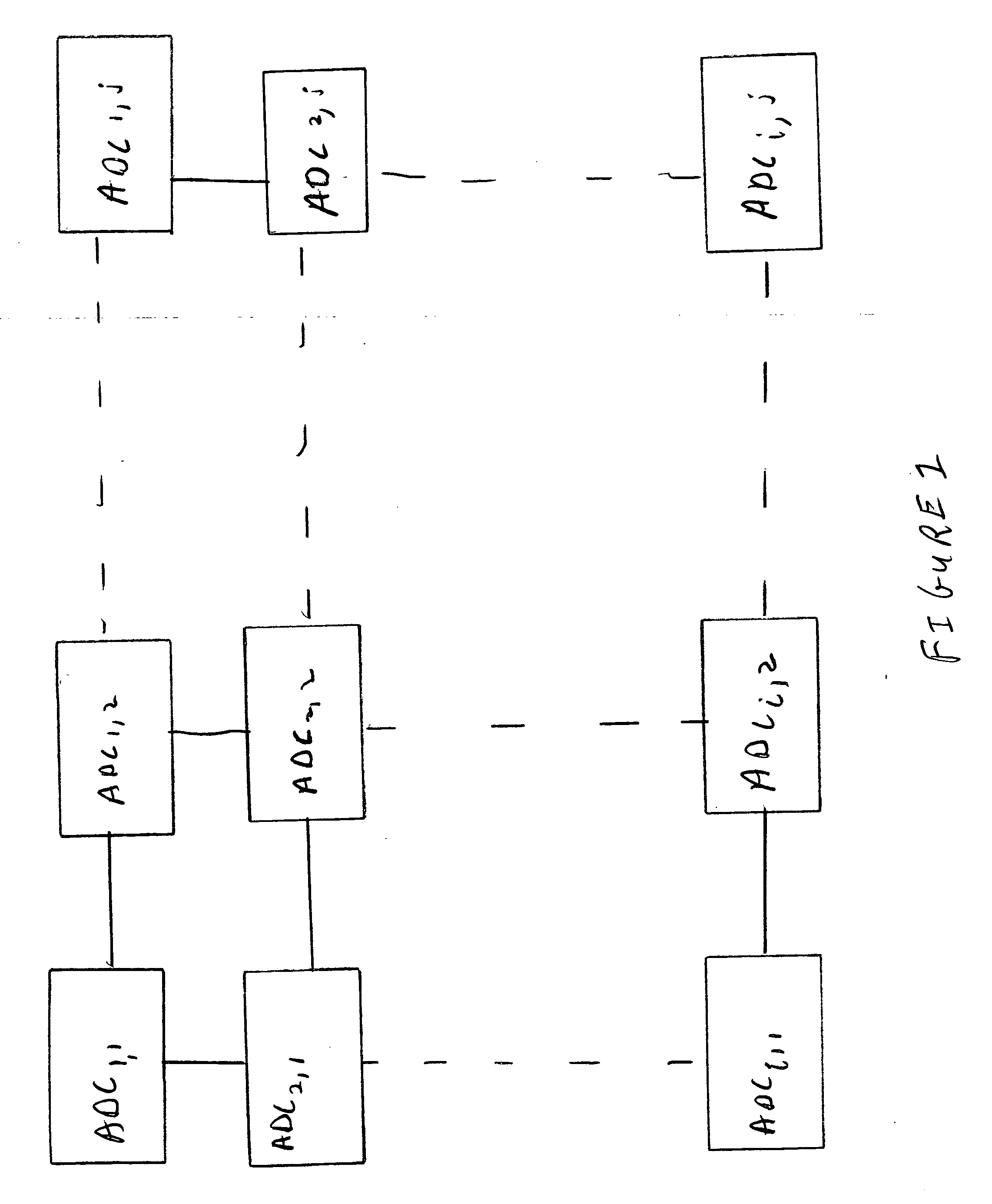
digital number (DN) that is proportional to the total charge accumulated over the frame period. In this illustrative embodiment, the DN for each pixel is then shifted to the edge of the ROIC and multiplexed with other DNs associated with other pixels for transfer off the array. By digitizing the
signal while photoelectrons are being collected, rather than after charge accumulation, the need for large charge storage capacitors and highly linear analog
electronics can be eliminated. The power dissipation and
noise problems associated with a conventional, analog readout, approach are also greatly reduced. Additionally, this approach permits operation with circuitry that operates from a lower level power supply, because the
dynamic range requirements associated with conventional systems needn't be maintained. Permitting operation with lower-level power supplies permits the use of
Integrated Circuit processes that offer much smaller feature sizes, thereby further enabling the ADC and readout circuitry to be packed within an area less than or equal to the area consumed by the associated detector
pitch, also referred to as the pixel
pitch. Simplifying the unit cell
preamplifier offers considerable power savings for large arrays.
[0013] In this illustrative embodiment, the
capacitor size defines the
least significant bit of the ADC. In this way, the size of the
capacitor may be kept to a minimum, thereby significantly reducing the area required for the
analog to digital conversion. In this illustrative embodiment, the
analog to digital conversion is achieved via a
voltage-to-frequency converter in which a predetermined amount of
photocurrent charges the capacitor to a level that produces an output pulse and resets the capacitor. The output pulses are counted and the count in a given time period corresponds to the amount of
photocurrent and, correspondingly, the
light flux impinging on the associated photodiode. In this way, the illustrative embodiment of a DFPA in accordance with the principles of the present invention digitizes the
signal while photoelectrons are being collected, rather than after charge accumulation.

