Photoresist coating system and method

a coating system and photoresist technology, applied in the direction of superimposed coating process, liquid/solution decomposition chemical coating, instruments, etc., can solve the problems of reducing affecting the yield of semiconductors, and even more serious edge bead problems, etc., to achieve the effect of uniform spread

Inactive Publication Date: 2007-04-05
SAMSUNG ELECTRONICS CO LTD
View PDF1 Cites 7 Cited by
  • Summary
  • Abstract
  • Description
  • Claims
  • Application Information

AI Technical Summary

Benefits of technology

[0021] To at least overcome the above problems, embodiments of the present invention provide at least a photoresist coa...

Problems solved by technology

Accordingly, in this environment, the edge bead problem may be even more serious.
However, if the photoresist coated on the wafer protrudes at the edge of the wafer, this protrusion...

Method used


Image

  • Photoresist coating system and method
  • Photoresist coating system and method
  • Photoresist coating system and method

Examples


Embodiment Construction

[0069] Reference will now be made in detail to embodiments of the present invention, examples of which are illustrated in the accompanying drawings, wherein like reference numerals refer to the like elements throughout. Embodiments are described below to explain the present invention by referring to the figures.

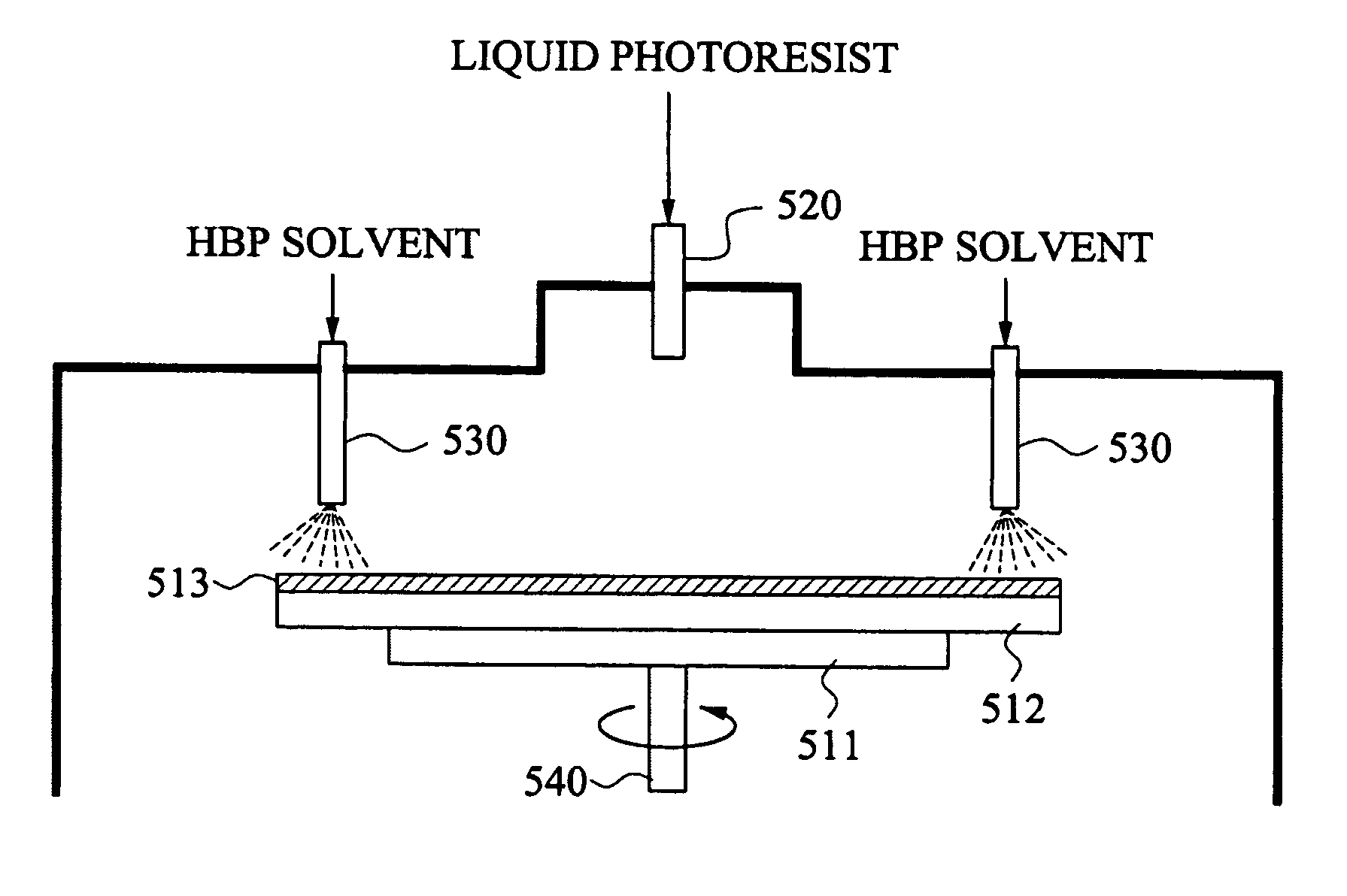
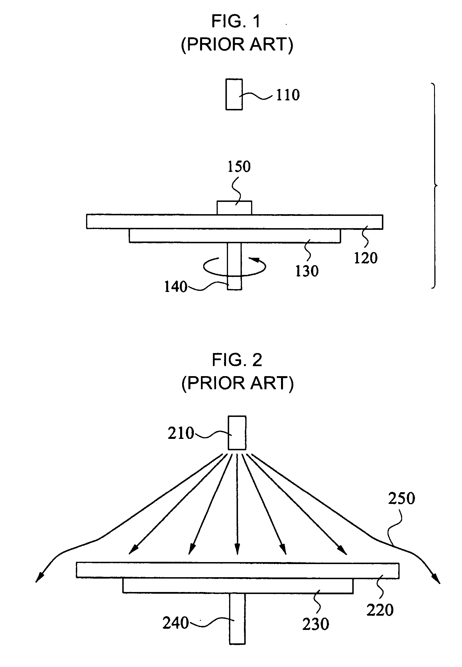
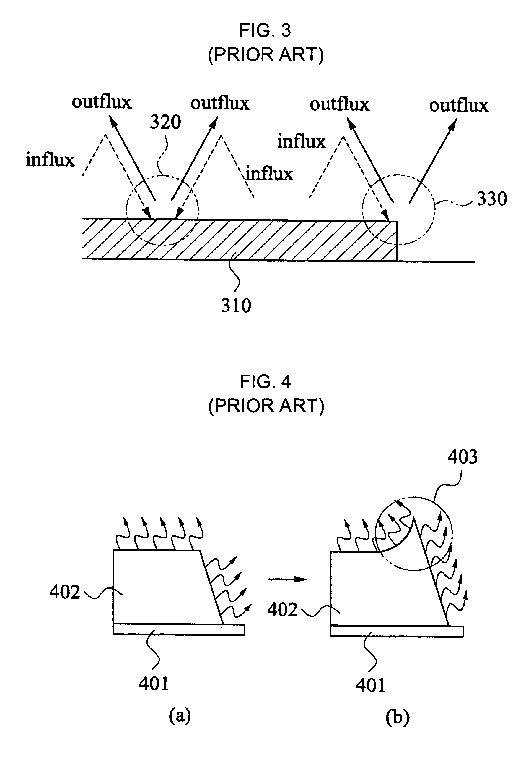
[0070] A photoresist coating system, according to an embodiment of the present invention may include different features, depending upon the materials available for supply to the edge of a wafer, e.g., adding a high boiling point (HBP) solvent or surfactant to the edge of the wafer. As noted above, the photoresist coating system may further include the additional features of adding spinning or additional spraying to evenly deposit liquid photoresist over a wafer.

[0071]FIG. 5 illustrates a photoresist coating system, according to an embodiment of the present invention. Here, the photoresist coating system may include a wafer substrate 511, a wafer 512, a photoresist nozzle (P...


PUM

PropertyMeasurementUnit
Boiling pointaaaaaaaaaa
Hydrophobicityaaaaaaaaaa

Abstract

A photoresist coating system and method solving an edge bead problem that occurs in photoresist coating by adding at least one of high boiling point solvent, which may generate a film on the surface of a solvent having a higher boiling point than a solvent contained in a liquid photoresist or the surface of the liquid photoresist, or by supplying a surfactant to an edge of the wafer, with the surfactant being combinable with the solvent or capable of forming a film on the solvent.

Description

CROSS-REFERENCE TO RELATED APPLICATIONS [0001] This application claims the priority benefit of Korean Patent Application No. 10-2005-93498, filed on Oct. 5, 2005, in the Korean Intellectual Property Office, the disclosure of which is incorporated herein by reference. BACKGROUND OF THE INVENTION [0002] 1. Field of the Invention [0003] Embodiments of the present invention relate to a photoresist coating system and method, and more particularly, to a photoresist coating system and method solving, in at least an embodiment of the present invention, an edge bead problem which occurs in photoresist coating by forming a film on the surface of a solvent having a higher boiling point than a solvent contained in a liquid photoresist or the surface of the liquid photoresist, and / or by supplying a surfactant to an edge of the wafer, the surfactant being combinable with the solvent, for example. [0004] 2. Description of the Related Art [0005] Photoresist coating is a process which is widely used...

Claims


Application Information

Patent Timeline
IPC IPC(8): B05D3/12B05D7/00B05C11/02B05B7/06
CPCG03F7/162G03F7/168G03F7/16
Inventor KOO, JUNEKIM, TAELEE, JINJUNG, CHANG
Owner SAMSUNG ELECTRONICS CO LTD
Why Eureka
Try Eureka