Method for preparing plasma display panel

a plasma display and plasma technology, applied in the manufacture of electrodes, electric discharge tubes/lamps, electromechanical systems, etc., can solve the problems of high-definition pdps, large screen size, and limited fine width of electrodes, so as to reduce manufacturing time and improve production efficiency. , the effect of reducing the manufacturing process

Inactive Publication Date: 2007-04-12
SAMSUNG SDI CO LTD
View PDF11 Cites 17 Cited by
  • Summary
  • Abstract
  • Description
  • Claims
  • Application Information

AI Technical Summary

Benefits of technology

[0008] An exemplary embodiment of the present invention provides a method of making a plasma display

Problems solved by technology

However, there is a limit for forming a fine width of electrodes, and the method

Method used


Image

  • Method for preparing plasma display panel
  • Method for preparing plasma display panel
  • Method for preparing plasma display panel

Examples


preparation example 2

Preparation of a Green Sheet

[0112] Another green sheet was prepared according to the same method as in Preparation Example 1, except for using a glass powder of B2O3—BaO—ZnO with an average particle diameter of 0.1 μm (comprising 70 wt % of B2O3, 15 wt % of BaO, and 10 wt % of ZnO) instead of the SiO2—ZnO—B2O3 glass powder.

preparation example 3

Preparation of a Green Sheet

[0113] A green sheet was prepared according to the same method as in Preparation Example 1, except for using a glass powder of Bi2O3—B2O3—SiO2—Al2O3—Na2O—MgO with an average particle diameter of 5 μm (25 wt % of Bi2O3, 25 wt % of B2O3 30 wt % of SiO2, 15 wt % of Al2O3, 2 wt % of Na2O, and 3 wt % of MgO) instead of the SiO2—ZnO—B2O3 glass powder.

example 1

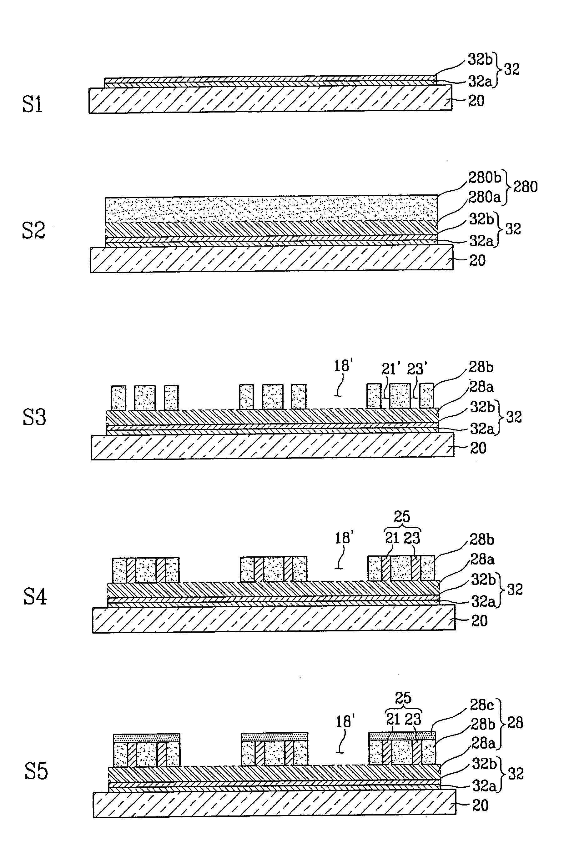
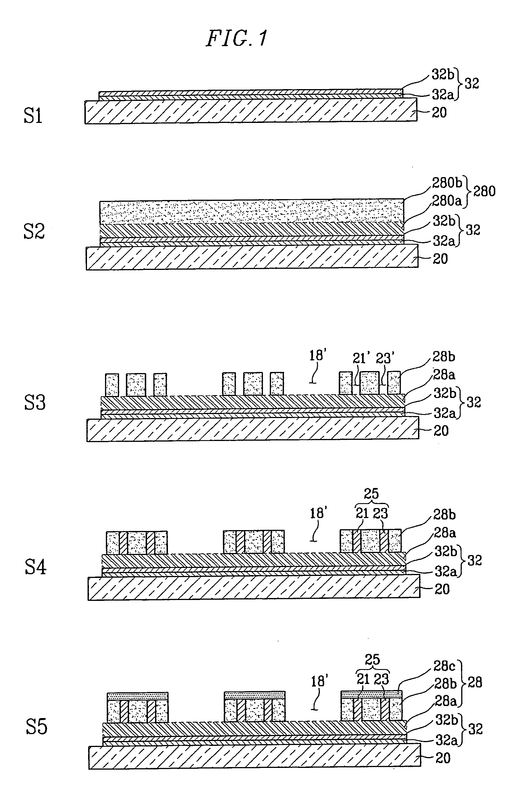
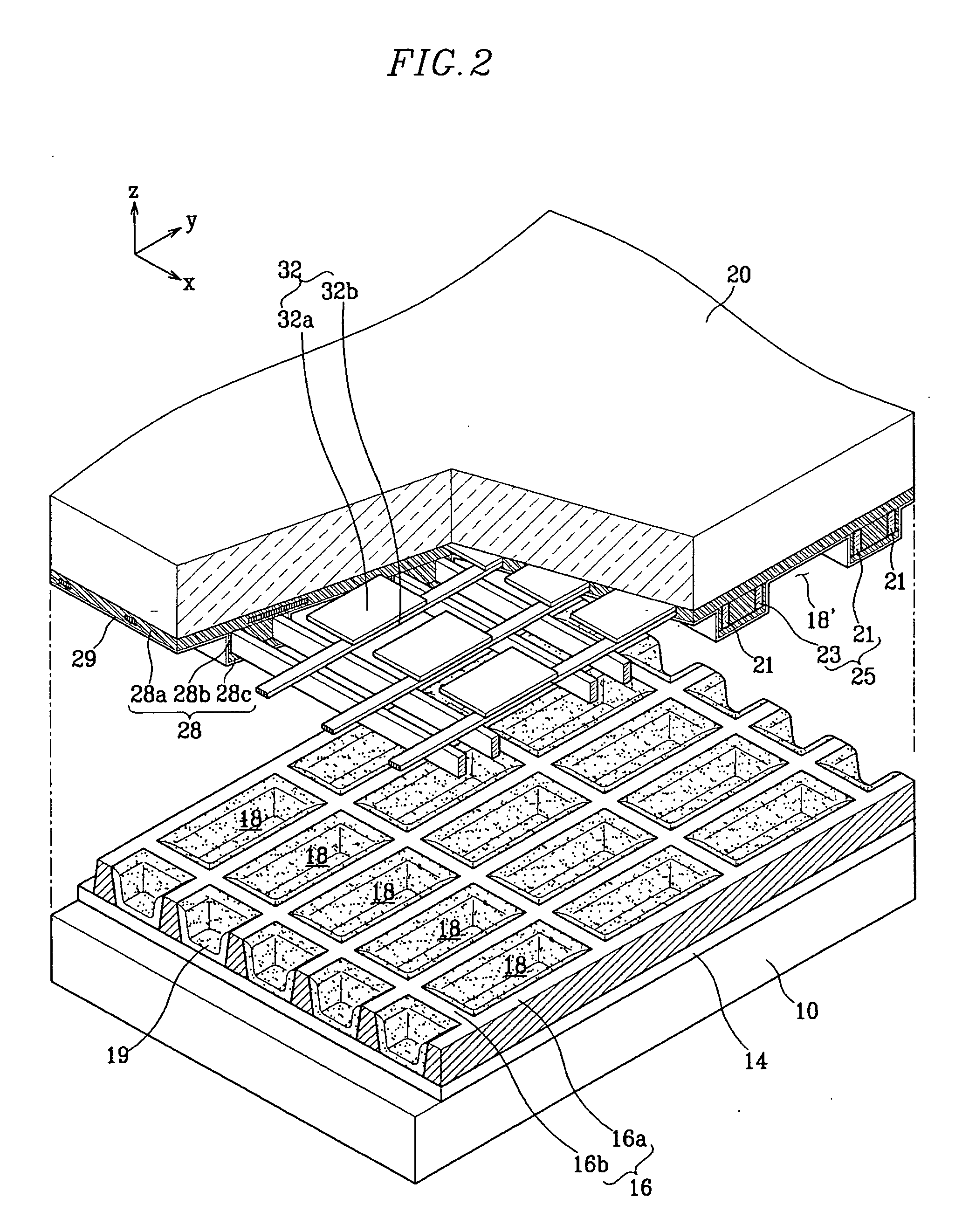
Manufacture of a Plasma Display Panel

[0114] A front substrate made of soda lime glass was sputtered with indium tin oxide and a dry film register (DFR) was laminated thereon. A patterned photo mask was additionally laminated on the DFR, and thereafter it was exposed by using high pressure mercury lamp, developed by using a 0.4% Na2CO3 alkali aqueous solution, and dried to pattern the DFR to have a shape corresponding to a protrusion electrode. Then, protrusion electrodes were formed by etching the patterned substrate with hydrochloric acid and nitric acid, peeling the DFR patterned part with an aqueous solution containing 5.0% of NaOH, and then firing it. A photosensitive paste for forming a bus electrode including Ag was applied on the protrusion electrodes. The coated photosensitive paste including Ag was leveled, dried, and thereafter exposed by using a DI (direct imaging) exposer. Next, bus electrodes having a stripe pattern were formed by repeating drying and exposing five tim...


PUM

PropertyMeasurementUnit
Temperatureaaaaaaaaaa

Abstract

A method of making a plasma display panel, whereby an address electrode is formed on a front substrate, a green sheet is formed to cover the address electrode, a dielectric layer pattern is formed by exposing, developing, and firing the green sheet, a composition for a display electrode is filled in the dielectric layer pattern and then fired to form a patterned display electrode, and a dielectric layer is formed to cover the patterned display electrode, thereby fabricating a front substrate. The green sheet includes a first green sheet that is formed using a dielectric composition, and a second green sheet that is formed on the first green sheet and using a photosensitive dielectric composition.

Description

CLAIM OF PRIORITY [0001] This application makes reference to, incorporates the same herein, and claims all benefits accruing under 35 U.S.C. §119 from an application earlier filed in the Korean Intellectual Property Office on 7 Oct. 2005 and there duly assigned Serial No. 10-2005-0094251. FIELD OF THE INVENTION [0002] The present invention relates to a method of making a plasma display panel. More particularly, the present invention relates to a method of making a plasma display panel in which a dielectric layer to cover an address electrode and a dielectric layer covering display electrodes are formed in a singular process using a two-layer green sheet, and which thereby simplifies a manufacturing process and reduces manufacturing time and inferior products. BACKGROUND OF THE INVENTION [0003] A plasma display panel (herein referred to as a “PDP”) is a display apparatus using plasma discharge. Vacuum ultraviolet (herein referred to as “VUV”) rays emitted by the plasma discharge exci...

Claims


Application Information

Patent Timeline
IPC IPC(8): H01J9/00H01J9/02H01J11/12H01J11/14H01J11/16H01J11/22H01J11/24H01J11/26H01J11/32H01J11/34H01J11/36H01J11/38H01J11/40H01J11/42
CPCC03C3/091C03C3/093C03C3/142C03C12/00C03C14/00C03C2214/12H01J9/02H01J11/14H01J11/38
Inventor SHIN, HYEA-WEONKIM, JEONG-NAMHWANG, YONG-SHIKKIM, MYOUNG-SUPCHOI, YOUNG-DO
Owner SAMSUNG SDI CO LTD
Why Eureka
Try Eureka