Image sensor mounted by mass reflow

a semiconductor image and mass reflow technology, applied in semiconductor devices, semiconductor/solid-state device details, radiation control devices, etc., can solve the problems of deteriorating productivity, time delay, weak mechanical resistance and heat resistance of inorganic matter formed on the surface of semiconductor devices,

Inactive Publication Date: 2007-04-19
NEPES CO LTD
View PDF4 Cites 15 Cited by
  • Summary
  • Abstract
  • Description
  • Claims
  • Application Information

AI Technical Summary

Benefits of technology

[0025] In a second embodiment to achieve the object of the present invention, there is provided a fabrication method of a structure of a package for a semiconductor image pickup device, comprising the steps of: forming an insulating film on the surface of a semiconductor image pickup device and then selectively etching the insulating film so as to expose electrode pads formed on the edges of the semiconductor image pickup device; forming at least one functional polymer layer on an image sensing unit formed at the center of the semiconductor image pickup device; forming a stress preventing polymer layer on the image sensing unit where the functionally polymer layer is formed; forming at least one m...

Problems solved by technology

Further, there is another problem that a wire bonding process, a plastic molding process, a ceramic process, etc. are needed in order to fabricate the package for the semiconductor image pickup device by means of wire bonding, which causes a time delay and deteriorates the productivity.
At this time, the inorganic matters, such as polymer, formed on the surface of the semiconductor device are weak in mechanical resistance and heat resistance in comparison with ceramic materials, such as the above-mentioned silicon nitride film or silicon oxide film.
At this time, the color filter layer is very weak in temperature condition and thus the properties thereof are deteriorated at a high temperature more than 250° C.
Further, the polymer layer comprised of a planarization layer, a color filter layer and a micro lens stacked on the surface of the semiconductor image pickup device may be deteriorated in mechanical strength even at a temperature of 250...

Method used


Image

  • Image sensor mounted by mass reflow
  • Image sensor mounted by mass reflow
  • Image sensor mounted by mass reflow

Examples


first embodiment

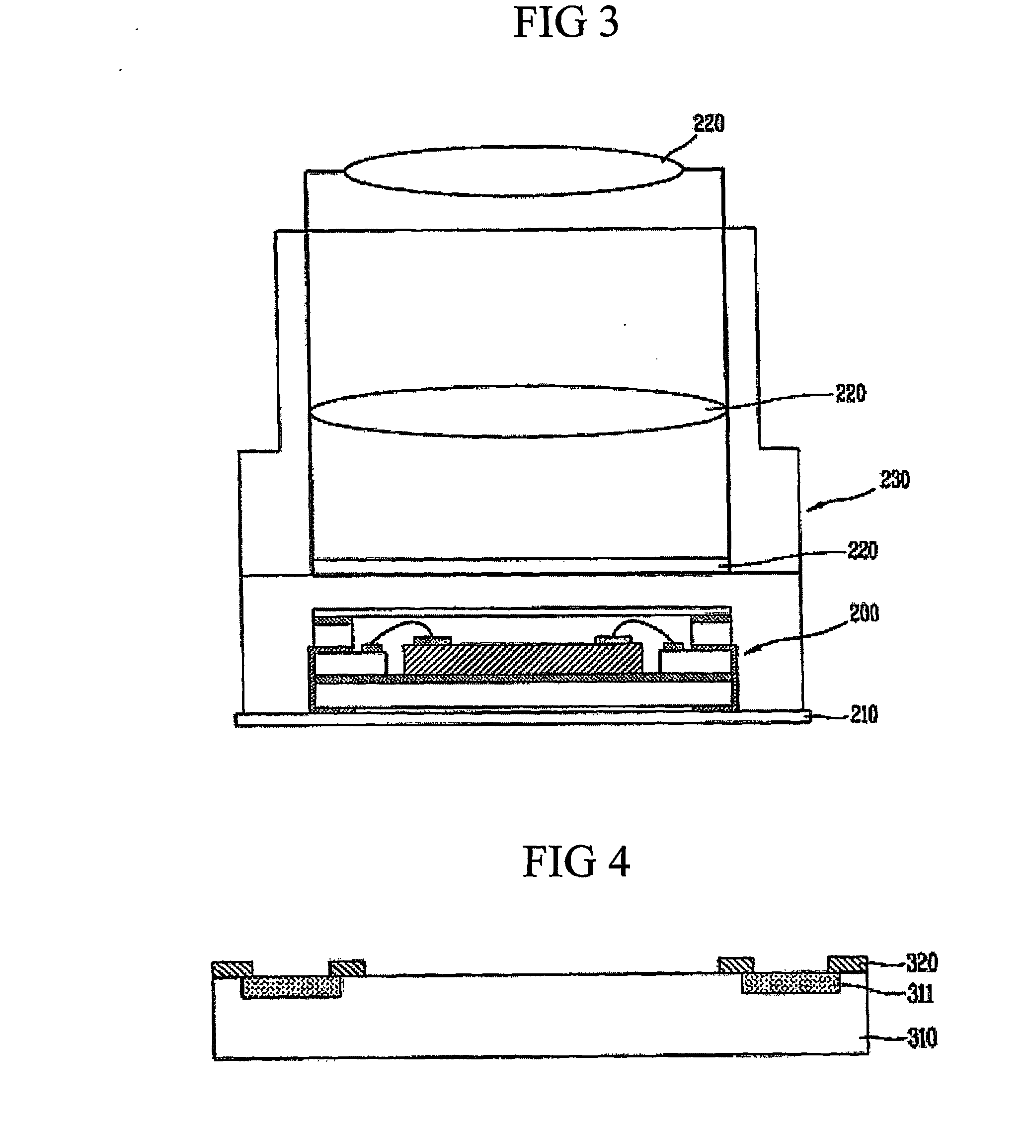
[0040] FIGS. 4 to 9 are exemplified views sequentially showing a fabrication method of a structure of a package for a semiconductor image pickup device in accordance with the present invention.

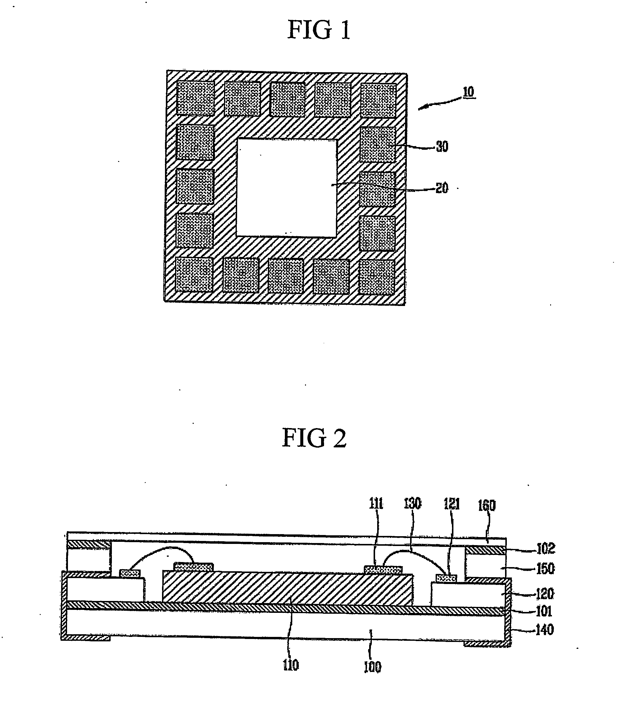
[0041] First, as shown in FIG. 4, an insulating film 320 is formed on the surface of a semiconductor image pickup device 310 and then the insulating film 320 is selectively etched so as to expose electrode pads 311 formed on the edges of the semiconductor image pickup device 310 and an image sensing unit (not shown) formed at the center of the semiconductor image pickup device 310.

[0042] As shown in FIG. 5, a functional polymer layer 330 is selectively formed on the image sensing unit formed at the center of the semiconductor image pickup device 310. At this time, as the functionally polymer layer 330, a planarization layer, a color filter layer and a micro lens are stacked so that the semiconductor image pickup device 310 have optical characteristics.

[0043] As shown in FIG. 6, a metallic bo...

second embodiment

[0059] FIGS. 14 to 21 are exemplified views sequentially showing a fabrication method of a structure of a package for a semiconductor image pickup device in accordance with the present invention.

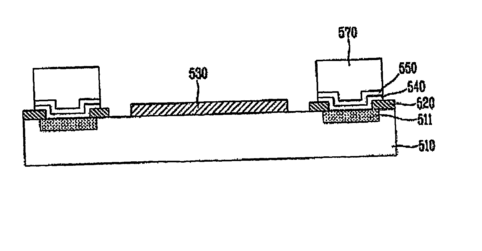
[0060] First, as shown in FIG. 14, an insulating film 520 is formed on the surface of a semiconductor image pickup device 510 and then the insulating film 520 is selectively etched so as to expose electrode pads 511 formed on the edges of the semiconductor image pickup device 510 and an image sensing unit (not shown) formed at the center of the semiconductor image pickup device 510.

[0061] As shown in FIG. 15, a functional polymer layer 530 is selectively formed on the image sensing unit formed at the center of the semiconductor image pickup device 510. At this time, as the functionally polymer layer 530, a planarization layer, a color filter layer and a micro lens are stacked so that the semiconductor image pickup device 510 have optical characteristics.

[0062] As shown in FIG. 16, a stress...


PUM


Abstract

A package for semiconductor image pickup device is provided. The package is fabricated by using flip chip bumping. During deposition process of forming a metallic bonding layer and a metal layer for plating, a surface of a semiconductor image pickup device is maintained at the range between room temperature and 200° C. in accordance with a first embodiment. A polymer layer for preventing stress from generating can absorb stress generated during the deposition process in accordance with a second embodiment. According to the present invention, a functional polymer layer on the surface of a semiconductor image pickup device can be prevent from being deteriorated in its properties and from transforming at its surface.

Description

BACKGROUND OF THE INVENTION [0001] 1. Field of the Invention [0002] The present invention relates to a structure of a package for a semiconductor image pickup device and a fabrication method thereof, and more particularly, to a structure of a package for a semiconductor image pickup device which is suitable for preventing the optical characteristics of the package for the semiconductor image pickup device from being deteriorated due to a damage of the surface of the semiconductor image pickup device in case where the package for the semiconductor image pickup device is fabricated by using flip chip bumping, and a fabrication method thereof. [0003] 2. Description of the Background Art [0004] Generally, a semiconductor image pickup device is referred to as an image sensor chip or solid state image pickup device. They pick up the image of an object by means of a photoelectric transducer converting the image of an object into an electric signal and a charged-coupled device transmitting ...

Claims


Application Information

Patent Timeline
IPC IPC(8): H01L23/02H01L21/00H01L27/148H01L23/00
CPCH01L27/14618H01L27/1462H01L27/14621H01L27/14625H01L27/14685H01L27/14687H01L2224/48091H01L2224/48227H01L2924/00014H01L23/00H01L27/148
Inventor KIM, JONG-HEONSONG, CHI-JUNG
Owner NEPES CO LTD
Why Eureka
Try Eureka