Substrate processing method and substrate processing apparatus

Active Publication Date: 2007-04-19
SCREEN HLDG CO LTD
View PDF20 Cites 31 Cited by
  • Summary
  • Abstract
  • Description
  • Claims
  • Application Information

AI Technical Summary

Benefits of technology

[0021] Energy of a jet of droplets can be increased further by heating a gas used to generate a jet of drople

Problems solved by technology

Ashing using a plasma, however, has a problem that the surface of the wafer is damaged in a portion uncovered with the resist film (for example, an exposed oxide film).
However, because the surface of the resis

Method used


Image

  • Substrate processing method and substrate processing apparatus
  • Substrate processing method and substrate processing apparatus
  • Substrate processing method and substrate processing apparatus

Examples


Example

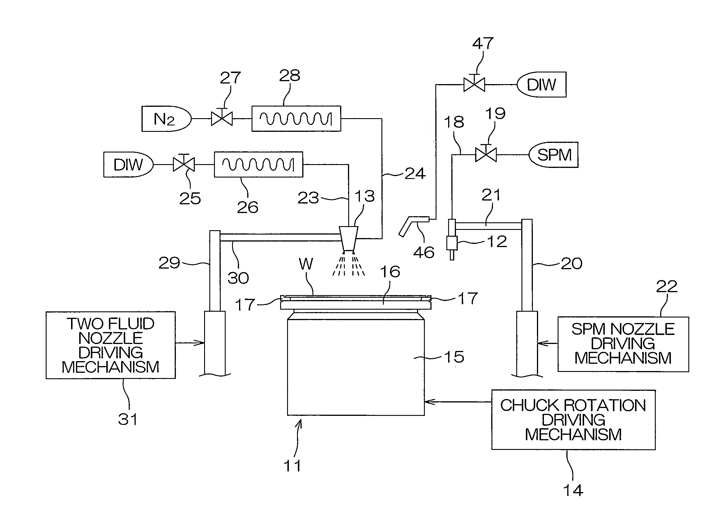
[0031]FIG. 1 is a view schematically showing a configuration of a substrate processing apparatus according to one embodiment of the invention.

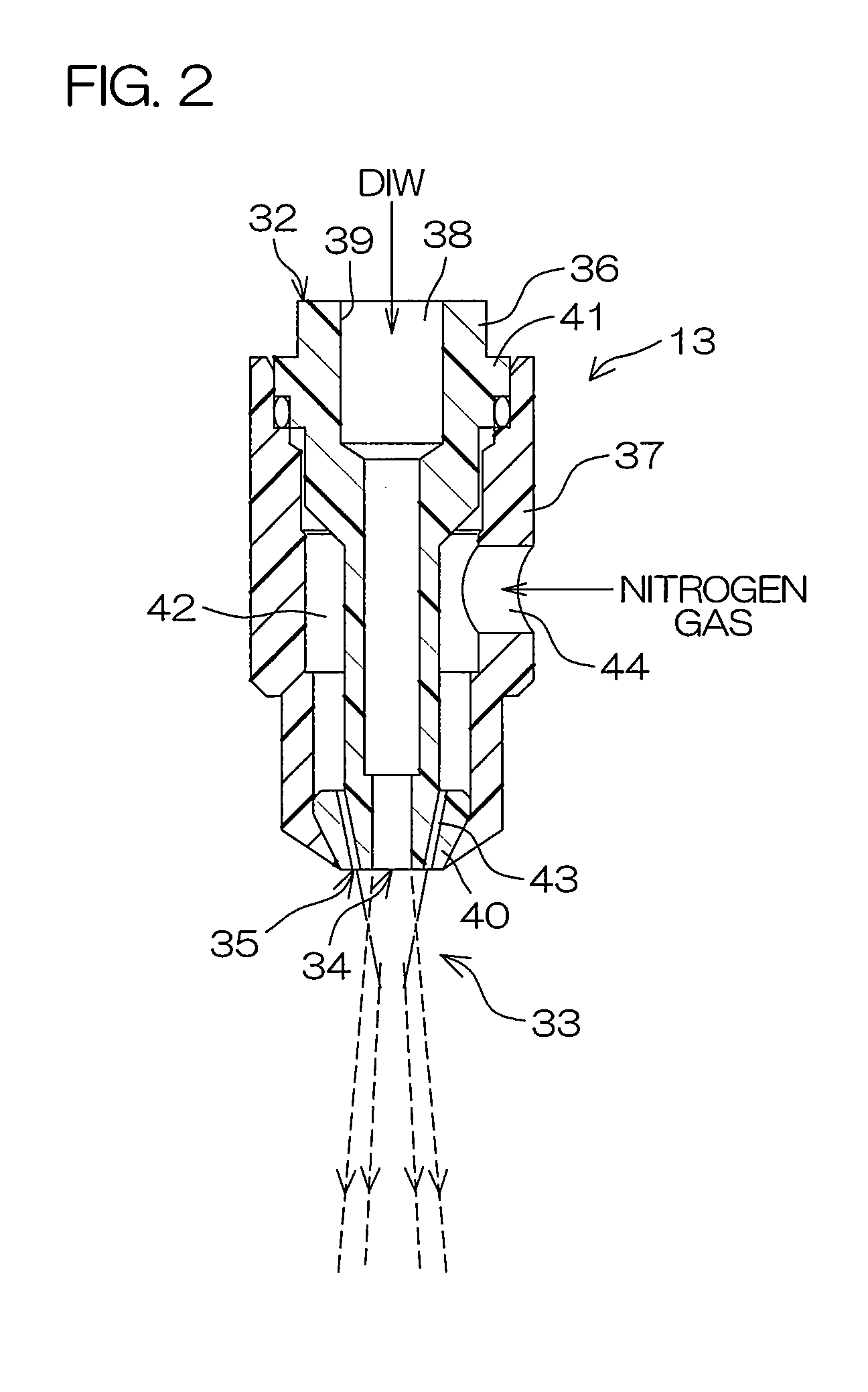
[0032] This substrate processing apparatus is, for example, an apparatus of a single substrate processing type that performs processing to remove unnecessary resist from the surface of a semiconductor wafer W (hereinafter, referred to simply as the wafer W) as an example of substrates by stripping after the ion implantation processing to implant impurities on the surface of the wafer W. The substrate processing apparatus includes a spin chuck 11 that rotates while holding the wafer W in almost a horizontal posture, an SPM nozzle 12 to supply SPM as a resist stripping liquid to the surface (top surface) of the wafer W held by the spin chuck 11, a two fluid nozzle 13 to supply a jet of droplets of heated DIW (deionized water) to the surface of the wafer W held by the spin chuck 11, and a DIW nozzle 46 to supply a continuous flow of DIW to the s...


PUM


Abstract

According to the substrate processing method of the invention, a jet of droplets generated from a gas and a heated processing liquid is supplied to the surface of a substrate. A resist stripping liquid to strip off the resist from the surface of the substrate is then supplied to the surface of the substrate.

Description

BACKGROUND OF THE INVENTION [0001] 1. Field of the Invention [0002] The present invention relates to a substrate processing method and a substrate processing apparatus applied to remove a resist from the surface of a substrate. The substrate includes a semiconductor wafer, a glass substrate for a liquid crystal display, a glass substrate for a plasma display, a glass substrate for an FED (Field Emission Display), an optical disc substrate, a magnetic disc substrate, a magneto-optical disc substrate, a photomask substrate, and so forth. [0003] 2. Description of Related Art [0004] The manufacturing process of a semiconductor device includes, for example, a step of locally implanting impurities (ions), such as phosphorous, arsenic, and boron, on the surface of a semiconductor wafer (hereinafter, referred to simply as the wafer). In this step, in order to prevent ions from being implanted in an undesired portion, a resist made of a photosensitive resin is formed in a pattern on the surf...

Claims


Application Information

Patent Timeline
IPC IPC(8): H01L21/00B41J2/045
CPCH01L21/67051H01L21/6708H01L21/304
Inventor HASHIZUME, AKIO
Owner SCREEN HLDG CO LTD
Why Eureka
Try Eureka