Semiconductor memory device, operational processing device and storage system

a memory device and memory technology, applied in the direction of information storage, static storage, digital storage, etc., can solve the problems of increasing the cost of design, development, production and distribution, long data holding time, short writing time, etc., and achieve the effect of fast and efficient operational processing

Inactive Publication Date: 2007-04-26
RENESAS ELECTRONICS CORP
View PDF3 Cites 54 Cited by
  • Summary
  • Abstract
  • Description
  • Claims
  • Application Information

AI Technical Summary

Benefits of technology

[0017] An object of the invention is to provide a semiconductor memory device that can achieve fast and efficient operational processing as well as an operational processing device and a memory system using such semiconductor memory device.
[0022] In the semiconductor memory device according to the invention, the plurality of memory regions store the information of different attributes, respectively, and the information is transferred via the buses that are selectively coupled. Therefore, the external operational processing device can access in parallel the information of different attributes such as processing data and an operational processing instruction, and can process in parallel the information of different attributes. Therefore, the processing efficiency of the external processing device can be improved.
[0023] The buses may be fixedly coupled to different ports, and the connection between the memory regions and the buses may be established according to port designating information, whereby the information of the same attribute can be transferred in parallel from each respective port, and the processing efficiency of the operational processing system can be improved.
[0025] The first and second memory regions have variable sizes, and can have their capacities optimized according to the capacities of the first and second memories. Therefore, it is possible to provide a cache system that can use the same construction for various purposes, so that the design efficiency of the system can be improved, and the manufacturing cost thereof can be reduced.
[0026] In the first operational processing unit according to the invention, the information is transferred between the plurality of data buses arid an external operational processing unit, and the information of different attributes can be transferred by accessing in parallel through the different buses, so that the instruction wait cycles can be reduced, and the operational processing system capable of fast processing can be implemented.
[0028] The capacities of the first and second memory regions can be readily changed according to the applications, and the operational processing unit that can flexibly accommodate for different purposes can be implemented.

Problems solved by technology

For example, when a mask ROM or a nonvolatile semiconductor memory device (flash memory) that can allow electrical programming and flash erasure is used for the ROM, if storage capacities of such memories is optimized, depending on individual purposes, in system designing, it is required to design memory device systems for each different processing application, resulting in an increased cost in the design, development, production and distribution.
As compared with the flash memory, FeRAM and MRAM have such features that writing requires a short time, a data holding time is long and the number of rewriting is greatly large.
Accordingly, an operational processing unit accessing this memory device cannot access in parallel the ROM and RAM regions, and instruction fetch cannot be performed in the same cycle as processing data transfer.

Method used


Image

  • Semiconductor memory device, operational processing device and storage system
  • Semiconductor memory device, operational processing device and storage system
  • Semiconductor memory device, operational processing device and storage system

Examples


first embodiment

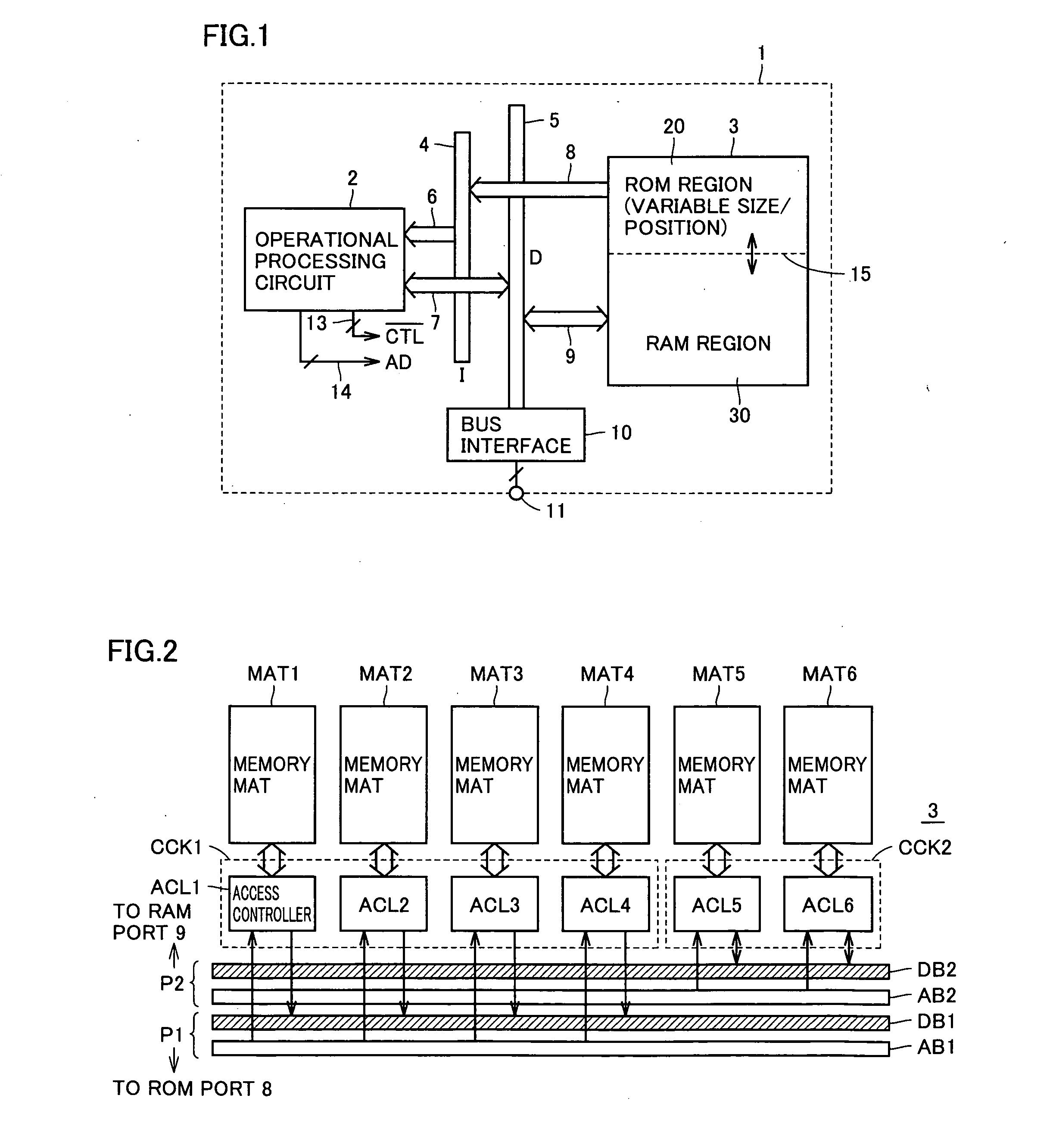
[0086]FIG. 1 schematically shows a whole construction of an operational processing system according to a first embodiment of the invention.

[0087] In FIG. 1, an operational processing system 1 according to the first embodiment of the invention includes an operational processing circuit 2 for executing operational processing / control processing according to received programs, and a semiconductor memory device 3 for storing program instructions and processing data for operational processing circuit 2.

[0088] Semiconductor memory device 3 is formed of a nonvolatile RAM such as an MRAM, and includes an ROM region 20 having storage information inhibited from being rewritten, and an RAM region 30 having stored information permitted to be rewritten. A boundary region (boundary address) 15 between ROM and RAM regions 20 and 30 is variable. The size and the position in the address space of ROM region 20 can be changed in the address space of nonvolatile RAM 3, and the physical position and st...

third embodiment

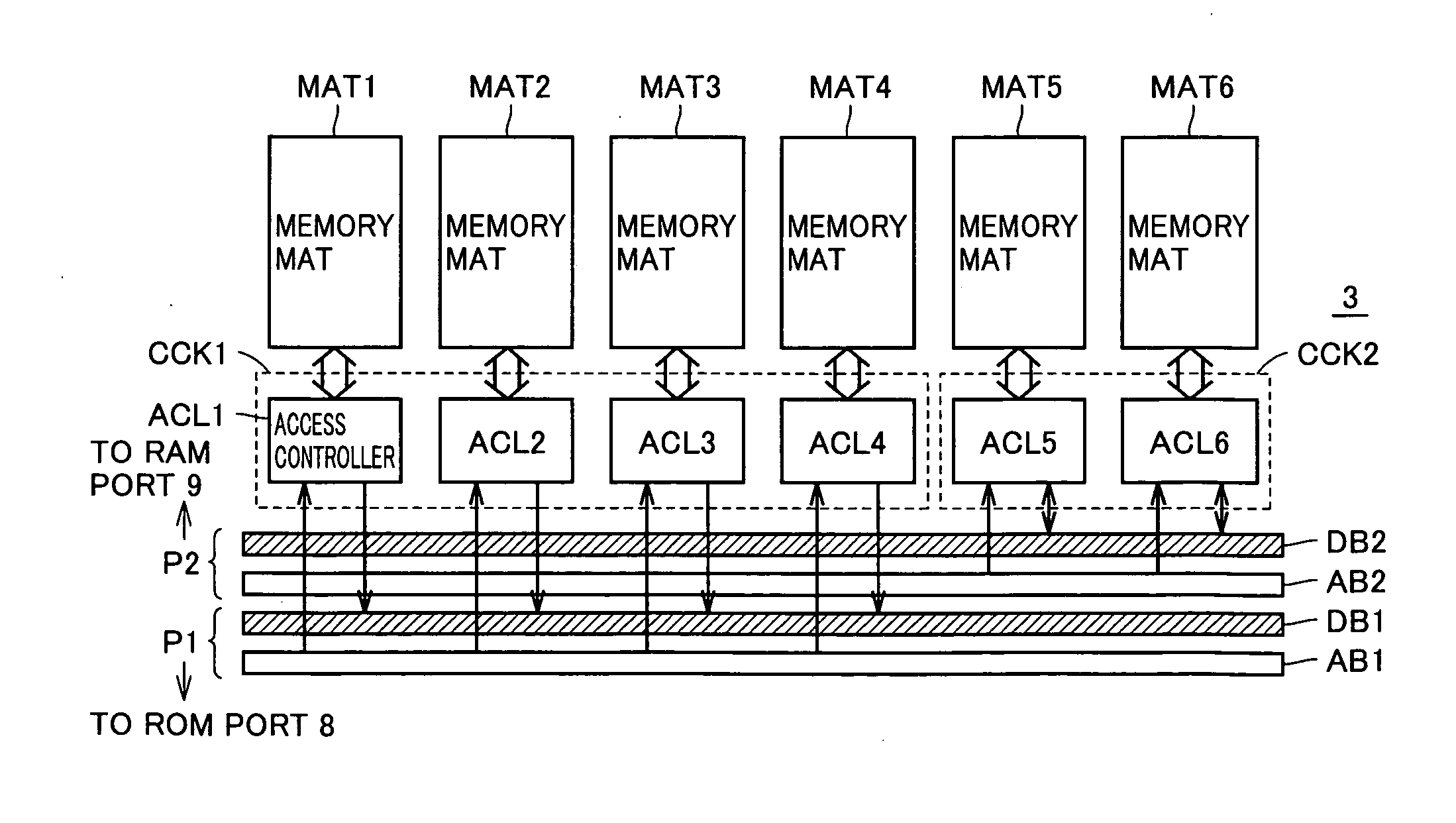
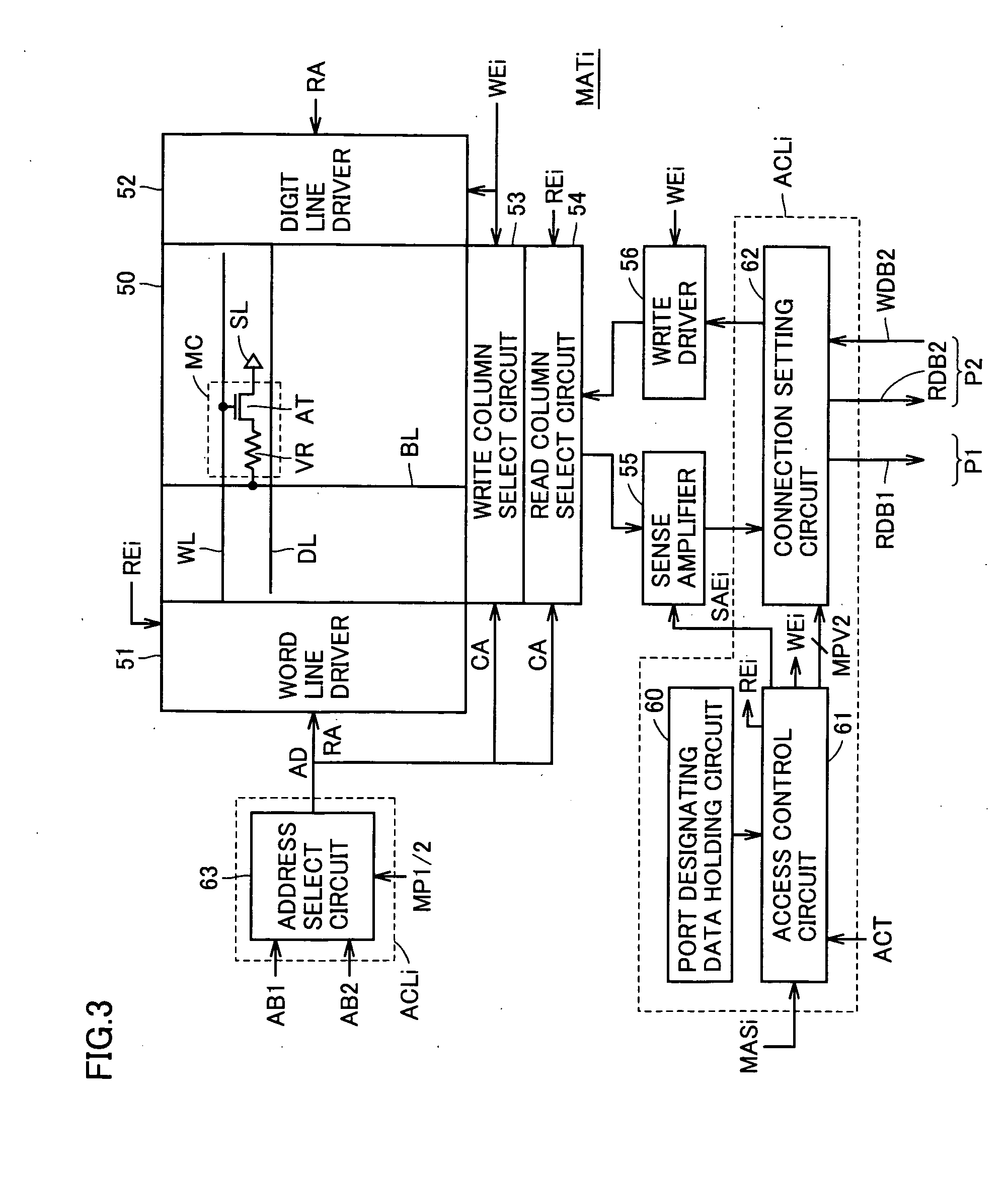
[0220]FIG. 18 schematically shows a whole construction of a nonvolatile RAM according to a third embodiment of the invention. In FIG. 18, the nonvolatile RAM includes M memory array blocks MAP1-MAPM. These memory array blocks MAP1-MAPM may be memory sub-blocks formed by dividing one memory cell array, respectively, or may be memory cell mats arranged individually and separately from each other on a common semiconductor chip. The memory cell mat is a memory circuit unit including an input structure, a column decoder and peripheral circuitry. In FIG. 18, memory array blocks MAP1-MAPM are arranged in one memory array, and is configured to share a digit line DL.

[0221] Each of memory array blocks MAP1-MAPM is divided into a plurality of I / O blocks. In FIG. 18, memory array block MAP1 includes I / O blocks I / O11-I / O1n, and memory array block MAP2 includes I / O blocks I / O21-I / O2-n.

[0222] Memory array block MAPM includes I / O blocks I / OM1-I / OMn. Each I / O block stores one bit of data / informati...

fourth embodiment

[0240]FIG. 20 schematically shows a construction of access controller ACLi according to a fourth embodiment of the invention. Access controller ACLi is arranged corresponding to each memory mat for setting the ROM and RAM regions. In the fourth embodiment, an operational processing circuit provided externally or on the same chip accesses each memory mat via ports P1 and P2, and whether these ports P1 and P2 are each used as the ROM port or the RAM port is set by port attribute setting signals ROM / RAM#1 and ROM / RAM#2. Port attribute setting signals ROM / RAM#1 and ROM RAM#2 set the corresponding ports as the RAM port when at H level. Therefore, in the fourth embodiment, one port is not fixed as the ROM port or as the RAM port, but can be flexibly and appropriately set as the ROM port or the RAM port according to the progress of processing or the contents of processing.

[0241] In FIG. 20, access controller ACLi includes an AND circuit 120a receiving an access instructing signal EN#1 (co...


PUM


Abstract

A thin film magnetic memory includes a size-variable Read Only Memory (ROM) region and a size-variable Random Access Memory (RAM) coupled to different ports for parallel access to the ports, respectively. A memory system allowing fast and efficient data transfer can be achieved.

Description

BACKGROUND OF THE INVENTION [0001] 1. Field of the Invention [0002] The present invention relates to a semiconductor memory device, an operational device and a memory system, and particularly to a memory device and memory system that can implement a processing system capable of fast operation. More particularly, the invention relates to a memory device, a processing system and a memory system using a Magnetic Random Access Memory (MRAM) in which an element such as a TMR (Tunneling MagnetoResistance) element or a MTJ (Magnetic Tunneling Junction) element utilizing a magnetoresistance effect, are employed for a memory element. [0003] 2. Description of the Background Art [0004] In a processing system using a processor such as a microprocessor or a microcontroller, a ROM (Read Only Memory) and a RAM (Random Access Memory) are employed as external memory devices. The ROM is used for storing fixed information such as control data and processing / control programs. The RAM is used as a worki...

Claims


Application Information

Patent Timeline
Patent Type & Authority Applications(United States)
IPC IPC(8): G11C8/00
CPCG11C11/005
Inventor HIDAKA, HIDETO
Owner RENESAS ELECTRONICS CORP
Why Eureka
Try Eureka