
Onboard data storage and method

a data storage and data technology, applied in the field of swallowable capsule cameras, can solve the problems of limiting the application of routine health screening tools, invasive and uncomfortable for patients, and the cost of these procedures, so as to save power and silicon area, simplify the address processing circuit, and simplify the interface from external to the semiconductor device.

Active Publication Date: 2007-04-26
CAPSO VISION INC
View PDF13 Cites 21 Cited by
  • Summary
  • Abstract
  • Description
  • Claims
  • Application Information

AI Technical Summary

Benefits of technology

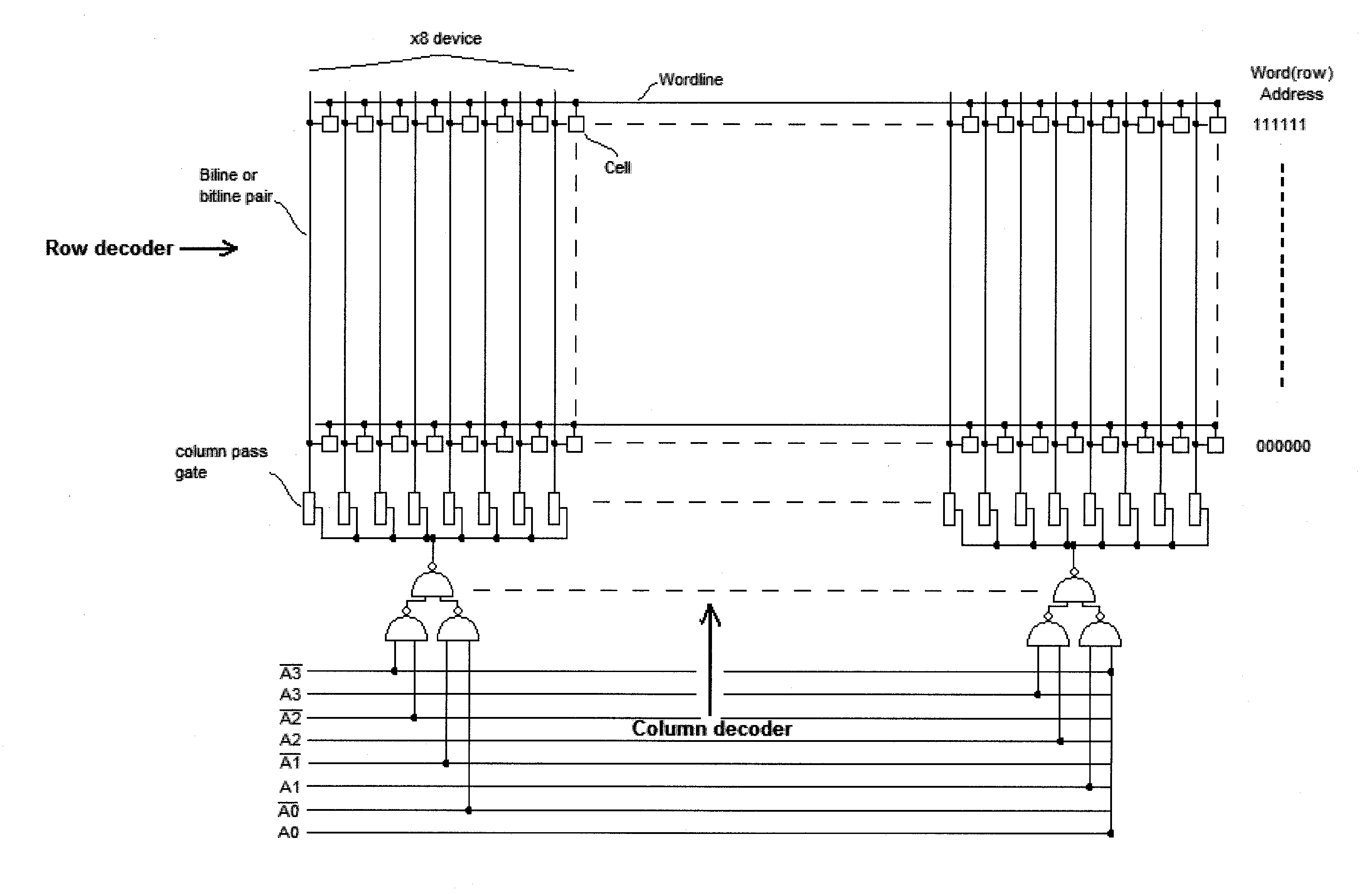
[0016] One embodiment of the present invention provides a semiconductor memory device and an associated method suitable for use in specific applications with predictable memory access pattern, such as in a capsule camera. The memory device takes advantage of the memory access pattern to simplify address processing circuit to realize savings in power and silicon area. Because random access to the semiconductor device is not required, the interface from external to the semiconductor device is also simplified by eliminating at least the address port that is used to specify the memory locations accessed. The present invention is applicable not only to non-volatile memory technologies (e.g., flash memory), it is also applicable to volatile memory technologies, such as transient charge storage-based memory circuits (e.g., DRAMs) and metastable states-based memory circuits (e.g., SRAMs).
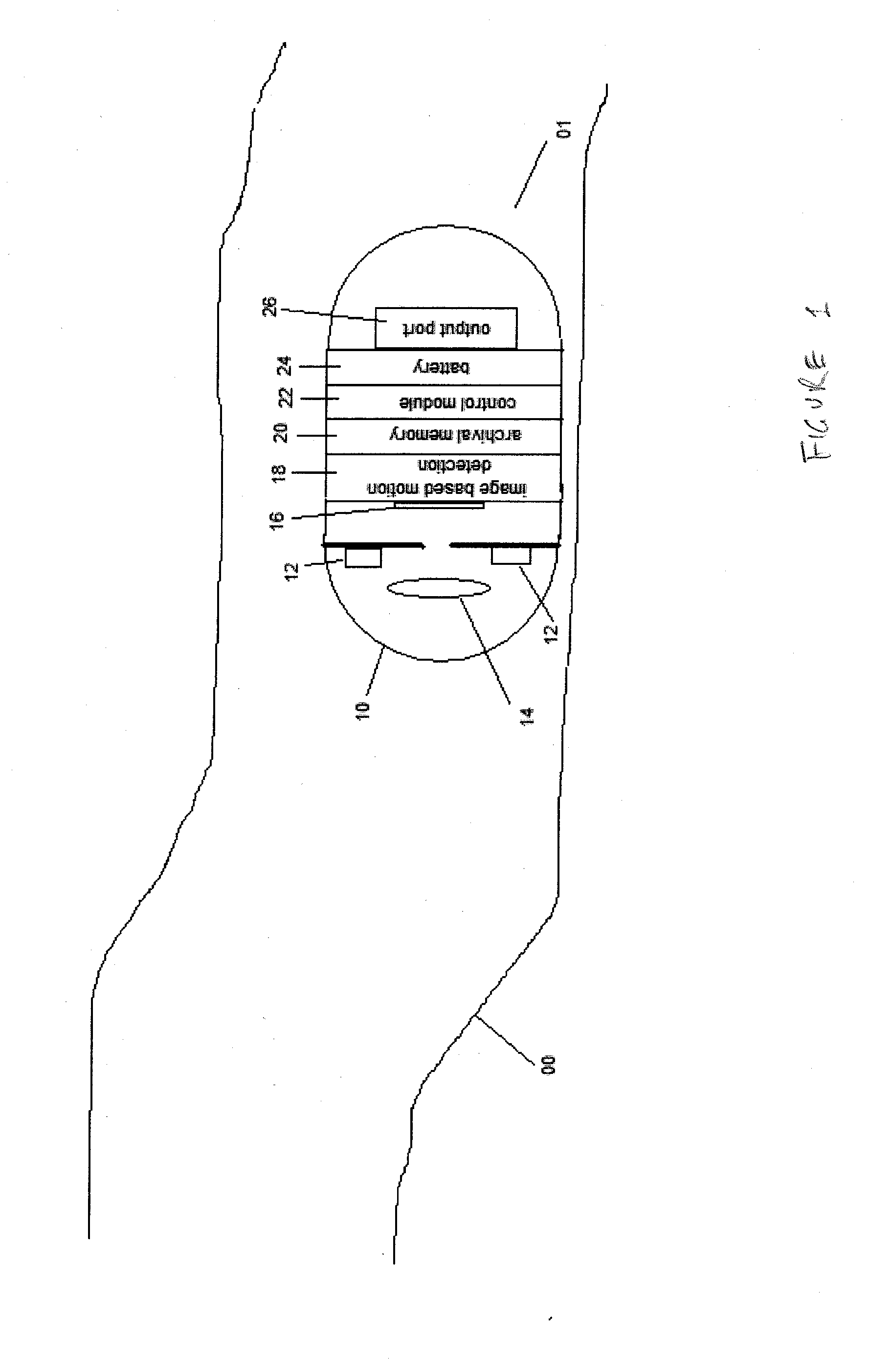
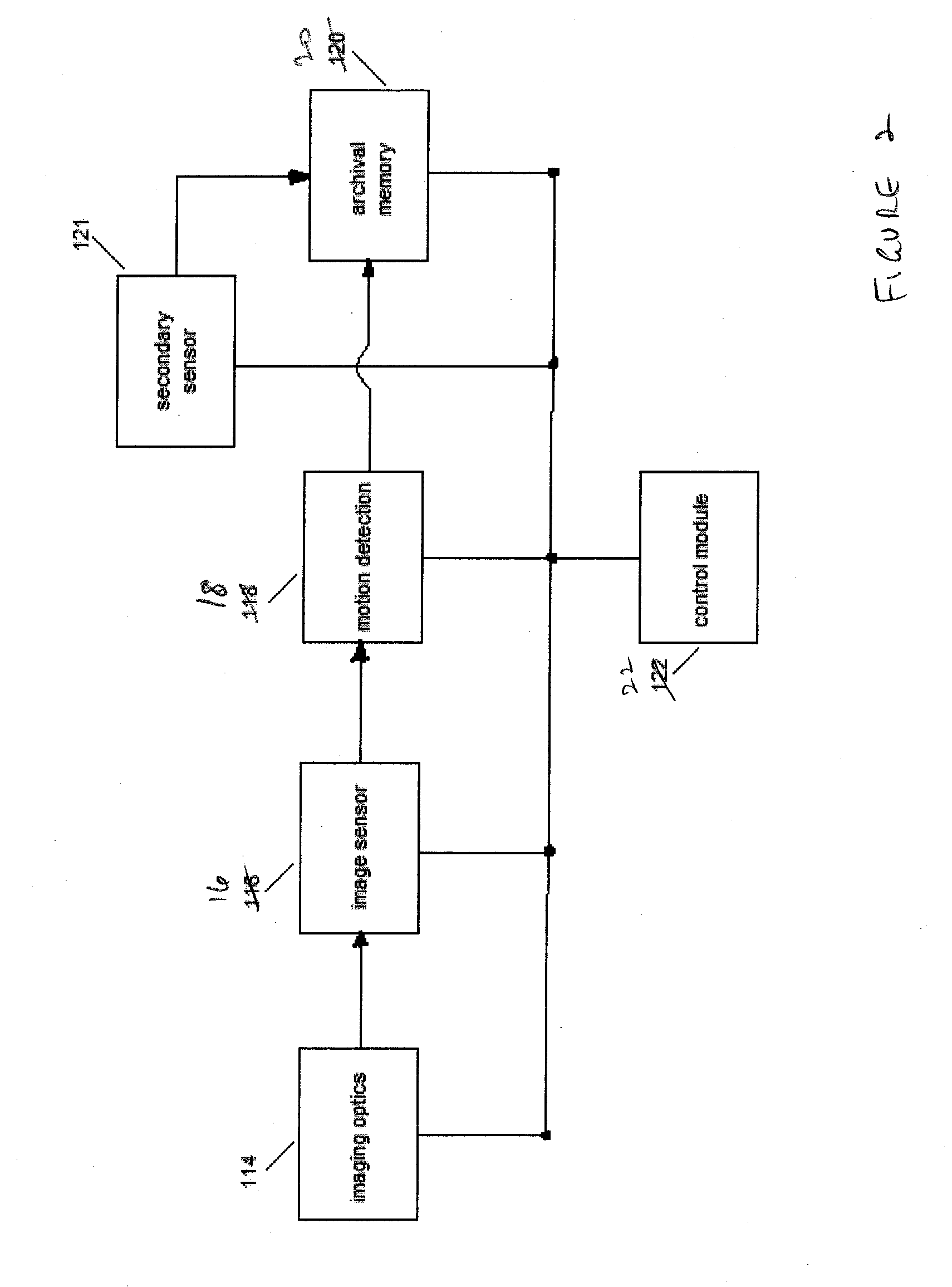
[0020] As mentioned above, the semiconductor memory device may be suitable for use in a capsule camera application. According to one embodiment of the present invention, the capsule camera may include a housing adapted to be swallowed, a light source within the housing, and a camera within the housing for capturing digital images of a scene illuminated by the light source. To maximize effectiveness of the space available in the semiconductor device, the capsule camera may further include a motion detector that detects a motion based on a difference between the digital images, and a motion evaluator that determines whether or not the storing later digital images is necessary. The predetermined memory access pattern eliminates a need for an address port that allows an external access device to specify memory locations. The interface to the semiconductor device is thereby greatly simplified, and facilitates an efficient design for accessing the semiconductor device to upload its contents.

Problems solved by technology

However, they have a number of limitations, present risks to the patient, are invasive and uncomfortable for the patient.
The cost of these procedures restricts their application as routine health-screening tools.
Because of the difficulty traversing a convoluted passage, endoscopes cannot reach the majority of the small intestine and special techniques and precautions, that add cost, are required to reach the entirety of the colon.
Endoscopic risks include the possible perforation of the bodily organs traversed and complications arising from anesthesia.
Moreover, a trade-off must be made between patient pain during the procedure and the health risks and post-procedural down time associated with anesthesia.
Endoscopies are necessarily inpatient services that involve a significant amount of time from clinicians and thus are costly.
The capsule camera allows the GI tract from the esophagus down to the end of the small intestine to be imaged in its entirety, although it is not optimized to detect anomalies in the stomach.
The cost of the procedure is less than for traditional endoscopy due to the decreased use of clinician time and clinic facilities and the absence of anesthesia.
However, these methods all require a physical media conversion during the data transfer process.
As a result, address decoding on a semiconductor memory device is a power-consuming operation.
In the current generation of semiconductor devices, such as a gigabit device, the complexity is significantly higher.

Method used


Image

  • Onboard data storage and method
  • Onboard data storage and method
  • Onboard data storage and method

Examples


Embodiment Construction

[0046] The Copending Patent Application discloses a capsule camera that overcomes many deficiencies of the prior art. Today, semiconductor memories are low-cost, low-power, easily available from multiple sources, and compatible with application specific integrated circuit (ASIC), sensor electronics (i.e., the data sources), and personal computers (i.e., the data destination) without format conversion devices. One embodiment of the present invention allows images to be stored in an “on-board storage” using semiconductor memories which may be manufactured using industry standard memory processes, or readily available memory processes. To optimize the use of the semiconductor memory device for diagnostic image storage, a method of the present invention may detect camera motion to control the number of images stored in the semiconductor memory device.

[0047] According to one embodiment of the present invention, a specialized frame buffer is provided. As a 640×480 resolution VGA-type ima...


PUM


Abstract

A semiconductor memory device and an associated method suitable for use in specific applications with predictable memory access pattern, such as in a capsule camera. The memory device takes advantage of the memory access pattern to simplify address processing circuit to realize savings in power and silicon area. Because random access to the semiconductor device is not required, the interface from external to the semiconductor device is also simplified by eliminating at least the address port that is used to specify the memory locations accessed. The method is applicable not only to non-volatile memory technologies (e.g., flash memory), it is also applicable to volatile memory technologies, such as transient charge storage-based memory circuits (e.g., DRAMs) and metastable states-based memory circuits (e.g., SRAMs).

Description

CROSS-REFERENCES TO RELATED APPLICATIONS [0001] The present invention is related and claims priority to (1) U.S. Provisional Patent Application, entitled “In Vivo Autonomous Sensor with On-Board Data Storage,” Ser. No. 60 / 730,797, filed on Oct. 26, 2005; (2) U.S. Provisional Patent Application, entitled “In Vivo Autonomous Sensor with On-Board Data Storage,” Ser. No. 60 / 739,162, filed on Nov. 23, 2005; (3) U.S. Provisional Patent Application, entitled “In Vivo Autonomous Sensor with Panoramic Camera,” Ser. No. 60 / 760,079, filed on Jan. 18, 2006; and (4) U.S. Provisional Patent Application, entitled “In Vivo Autonomous Sensor with On-Board Data Storage,” Ser. No. 60 / 760,794, filed on Jan. 19, 2006. These U.S. Provisional Patent Applications (1)-(4) (collectively, the “Provisional Patent Applications”) are hereby incorporated by reference in their entireties. The present application is also related to U.S. patent application (the “Copending Application”), entitled “In Vivo Autonomous ...

Claims


Application Information

Patent Timeline
IPC IPC(8): G11C8/00H04N5/225G03B41/00
CPCA61B1/0002A61B1/00036A61B1/041G03B37/005G11C7/1018G11C7/1021G11C8/04G11C8/08G11C16/10H04N5/2252A61B5/7232H04N23/51
Inventor WANG, KANG-HUAI
Owner CAPSO VISION INC
Learn More