Semiconductor device and method for fabricating the same

a semiconductor and polysilicon resistor technology, applied in semiconductor devices, solid-state devices, transistors, etc., can solve the problems of reducing the contact resistance between the resistance element and the plug, and it is difficult to simply fabricate a semiconductor device including the fusi electrode and the polysilicon resistor, and achieve good controllability

Inactive Publication Date: 2007-05-03
PANASONIC CORP
View PDF3 Cites 72 Cited by
  • Summary
  • Abstract
  • Description
  • Claims
  • Application Information

AI Technical Summary

Benefits of technology

[0008] In view of the foregoing, an object of the present invention is to provide a semiconductor device including a FUSI electrode and a polysilicon resistor and enabling a simple fabrication thereof, and to provide its fabrication method.
[0010] This structure of the device can prevent depletion of the first gate electrode occurring around the first gate insulating film, and also reduce the contact resistance between the resistance element and the plug. Moreover, the MIS transistor with a so-called FUSI electrode and the polysilicon resistor can be fabricated partly by common steps, which enables a simple fabrication of the semiconductor device.
[0012] In the case where an entire depthwise portion of the contact formation region of the resistance element is formed of the first silicide layer, the contact formation region can be silicided simultaneously with the first gate electrode. This inhibits expansion of the silicide layer into a portion to be a resistor, so that the resistor can be formed with good controllability.

Problems solved by technology

However, in the process flow for a FUSI electrode formation, the step of siliciding a diffusion layer and the step of siliciding a polysilicon gate electrode are conducted separately, so that it is difficult to simply fabricate a semiconductor device including the FUSI electrode and the polysilicon resistor.
This structure of the device can prevent depletion of the first gate electrode occurring around the first gate insulating film, and also reduce the contact resistance between the resistance element and the plug.

Method used


Image

  • Semiconductor device and method for fabricating the same
  • Semiconductor device and method for fabricating the same
  • Semiconductor device and method for fabricating the same

Examples


first embodiment

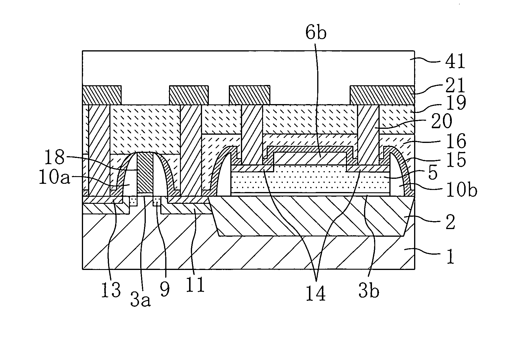
[0031]FIG. 1 is a sectional view showing a semiconductor device according to a first embodiment of the present invention. Referring to FIG. 1, the semiconductor device of the first embodiment is characterized in that the device includes a so-called FUSI electrode 18 and a polysilicon resistor with only a connection portion to a plug 20 and its vicinity silicided.

[0032] To be more specific, the semiconductor device of the first embodiment includes: a semiconductor substrate 1 made of silicon or the like; an isolation insulating film 2 surrounding an active region of the semiconductor substrate 1 and buried in the semiconductor substrate 1; a MIS (Metal-Insulator-Semiconductor) transistor formed on the active region of the semiconductor substrate 1; and a resistance element having a polysilicon resistor 5 provided above, for example, the isolation insulating film 2 with a first insulating film 3b interposed therebetween. The resistance element is composed of: a resistor region made o...

second embodiment

[0053]FIG. 5 is a sectional view showing a semiconductor device according to a second embodiment of the present invention. The semiconductor device of the second embodiment differs from the semiconductor device of the first embodiment in that of a polysilicon resistor 5, a silicide layer 45 for the resistor provided in a contact formation region is silicided to the bottom.

[0054] To be more specific, the semiconductor device of the second embodiment includes: a semiconductor substrate 1 made of silicon or the like; an isolation insulating film 2 surrounding an active region of the semiconductor substrate 1 and buried in the semiconductor substrate 1; a MIS (Metal-Insulator-Semiconductor) transistor formed on the active region of the semiconductor substrate 1; and a polysilicon resistor 8 provided above, for example, the isolation insulating film 2 with a first insulating film 3b interposed therebetween. Note that the first insulating film 3b does not necessarily have to be formed be...

third embodiment

Modification of Third Embodiment

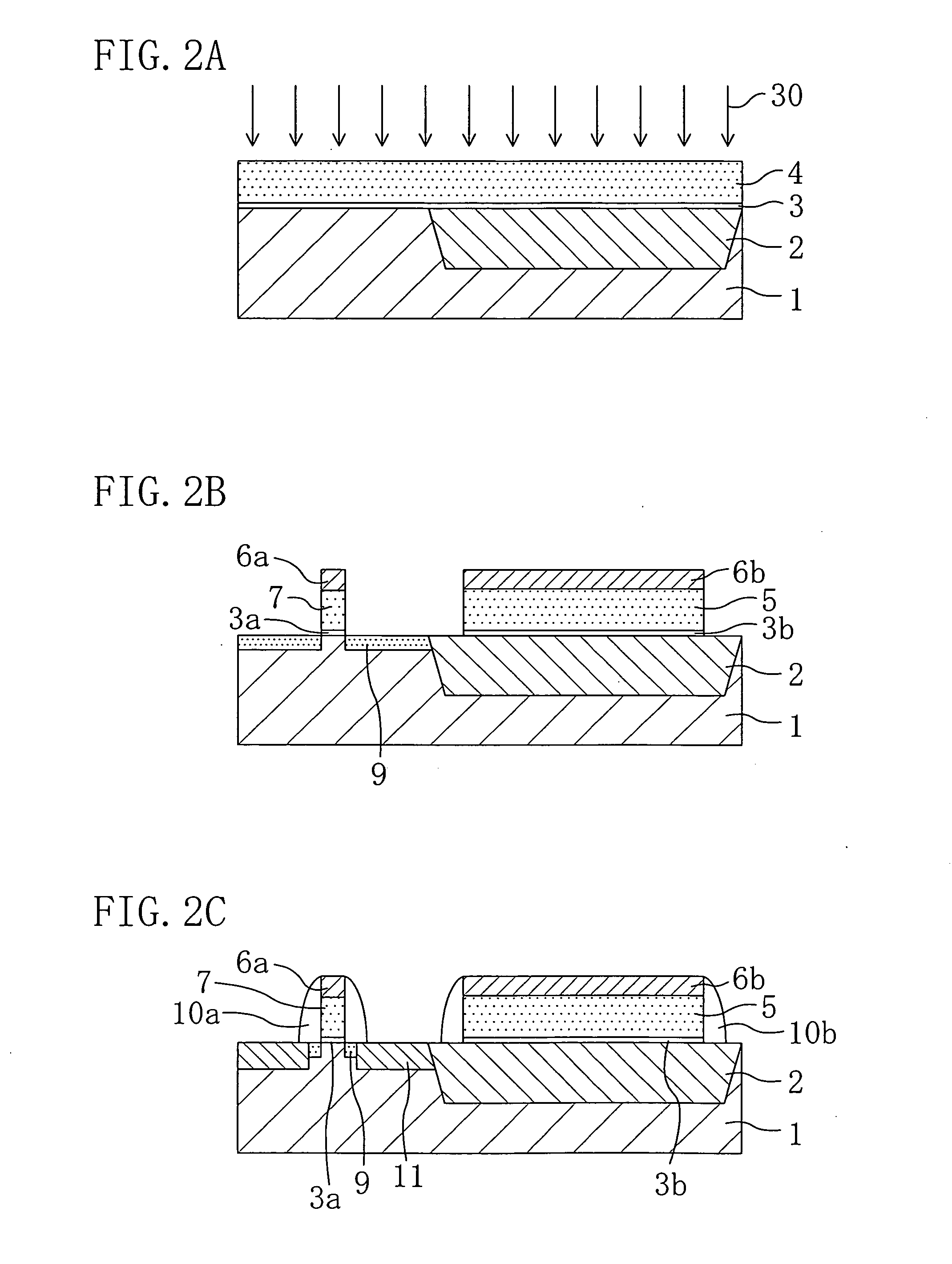
[0080]FIGS. 9A to 9C are sectional views showing a method for fabricating a semiconductor device according to one modification of the third embodiment of the present invention.

[0081] Referring to FIG. 9A, first, after the step shown in FIG. 8A, a Ni film 50a with a thickness of 49 nm is formed by a sputtering method or the like over the entire surface of the substrate.

[0082] Next, as shown in FIG. 9B, a mask 51 having an opening located only above the polysilicon resistor 5 is formed on the Ni film 50a, and then an exposed portion of the Ni film 50a is removed by etching. This procedure exposes the contact formation region of the polysilicon resistor 5.

[0083] Subsequently, as shown in FIG. 9C, after removal of the mask 51, a Ni film 50b with a thickness of 11 nm is formed by a sputtering method or the like over the entire surface of the substrate. In this modification, the Ni films 50a and 50b constitute the Ni film 50. This provides the semiconduc...


PUM


Abstract

In a semiconductor device including a MIS transistor with a FUSI gate electrode and a polysilicon resistor, a portion of the polysilicon resistor provided in a contact formation region is silicided simultaneously with the gate electrode or an impurity diffusion region.

Description

BACKGROUND OF THE INVENTION [0001] (a) Fields of the Invention [0002] The present invention relates to semiconductor devices and their fabrication methods. In particular, the present invention relates to semiconductor devices including FUSI (fully silicided) gate electrodes, and to their fabrication methods. [0003] (b) Description of Related Art [0004] In research and development of CMOS devices ever-increasingly miniaturized, active studies are being conducted to employ metal electrodes for the purpose of preventing depletion of gate electrodes. Among these studies, FUSI (fully silicided) gate electrodes are particularly proposed which are each made by fully siliciding a polysilicon electrode to form a silicide electrode. [0005] For these devices, if polysilicon with a relatively high resistance is used for a resistor, a process for attaining the state of connection of the polysilicon resistor to polycide with a low resistance is proposed in a conventional salicide process. [0006]F...

Claims


Application Information

Patent Timeline
Patent Type & Authority Applications(United States)
IPC IPC(8): H01L29/94H01L27/108H01L21/336H01L29/76H01L31/119
CPCH01L27/0251H01L27/0629H01L28/20
Inventor OGAWA, HISASHIKOTANI, NAOKIAKAMATSU, SUSUMUKUDO, CHIAKI
Owner PANASONIC CORP
Why Eureka
Try Eureka