Metal nanoparticle dispersion usable for ejection in the form of fine droplets to be applied in the layered shape

a metal nanoparticle and droplet technology, applied in the direction of electrically conductive paints, conductive pattern formation, other chemical processes, etc., can solve the problems of high thickness/width ratio, difficult to form a conductive metal paste coating, incident of voids, etc., to achieve high shape controllability, low impedance, and large film thickness

Active Publication Date: 2007-05-03
HARIMA CHEM INC +1
View PDF11 Cites 47 Cited by
  • Summary
  • Abstract
  • Description
  • Claims
  • Application Information

AI Technical Summary

Benefits of technology

[0009] As described above, along with narrowing of line widths of wiring used for a wiring pattern, which is formed on a substrate of wiring circuit, it is desired to develop a technique for forming a conductive wiring layer with wide applicability and high reproducibility, which may successfully increase the thickness / width ratio of a cross-section of the wiring layer employed, particularly in a narrow line portion. Particularly, in view of wider applicability in drawing of wiring patterns, it is desired to develop a technique for forming a conductive wiring layer with high reproducibility, which can increase the thickness / width ratio of a cross-section of the wiring layer by a coating process which requires no mask and in which droplets of a conductive metal paste dispersion are discharged and coated in line with the intended coating pattern by deposition or inkjet, instead of such a method using a beforehand prepared mask pattern as screen printing.
[0010] More specifically, when a conductive wiring layer is formed from a conductive metal paste dispersion in making of a wiring pattern having a fine minimum line width, be ultra-fine metal particles having an average particle size of several nm to several 10 nm need to be employed for the conductive medium (metal filler) used therein, in order to achieve drawing accuracy of fine line-width, for example, drawing accuracy and controllability of line width at sub-micron level. Specifically, it is desired to develop a technique for forming a conductive wiring layer with such a high thickness / minimum width ratio that a thickness of more than 10 μm is chosen finally for a minimum line width of less than 10 μm by means of drawing a coating layer by inkjet with use of a metal nanoparticle dispersion which contains, as a conductive medium, ultra-fine metal particles having an average particle size of several nm to several 10 nm in a dispersion solvent thereof, easily with high reproducibility. It is also desired to develop a metal nanoparticle dispersion having high fluidity suitably used for drawing of a coating layer having such a high thickness / minimum width ratio by inkjet.
[0011] The present invention has been made in order to solve the aforementioned problems, and an object of the present invention is to provide a dispersion of conductive metal paste type that employs only metal nanoparticles as a conductive medium, which is useful for forming an electroconductive layer having such an extremely fine pattern as a circular pattern having a diameter of several μm and a high thickness / minimum width ratio in the cross-section, and which has high fluidity adapted to successful application of inkjet when forming such fine pattern at high accuracy; and to provide a method for preparing an electroconductive layer having an extremely fine pattern and enough high thickness / minimum width ratio in the cross-section to exhibit excellent conductive properties, using said metal nanoparticle dispersion of conductive metal paste type. More specifically, an object of the present invention is to provide a metal nanoparticle dispersion having a novel constituent, which can form an extremely fine pattern and heighten the thickness / minimum width ratio in the cross-section to 1 / 1 or higher when a coating layer drawn in the shape of a fine wiring pattern using a metal nanoparticle dispersion is heat-treated at a low temperature to form an electroconductive layer of sintered product type in which the metal nanoparticles are sintered up at the low temperature; and which can achieve a superior conductive properties at high reproducibility that the specific resistivity of the resulted electroconductive layer of sintered product type having extremely fine pattern is within 10 times or preferably within 5 times the specific resistivity of the bulk of the metal material constituting said metal nanoparticles, and thus which is capable of producing a conductive body of fine sintered product type which possesses stably good conductive properties with high reliability.

Problems solved by technology

For example, in the case of metal plated films formed by means of electrolytic plating, metal is deposited even on the edges of the line when the line width is narrower and the plating thickness is increased; and therefore it is difficult to form a plated film having a narrow line width and a high thickness / width ratio with maintaining integrity of the desired finer wiring pattern.
Thus, it is also difficult to form a conductive metal paste coating layer having a narrow line width and a high thickness / width ratio with maintaining integrity of the desired finer wiring pattern.
In particular, when the proportion of the dispersion solvent contained in the used conductive metal paste is increased to obtain high fluidity, vapor of the dispersion solvent forms accidentally bubbles inside the opening groove at the stage of removing the dispersion solvent contained in the coating layer by evaporation after application, which may be a main cause resulting in incident of voids.

Method used


Image

  • Metal nanoparticle dispersion usable for ejection in the form of fine droplets to be applied in the layered shape
  • Metal nanoparticle dispersion usable for ejection in the form of fine droplets to be applied in the layered shape

Examples


reference examples 1 to 3

[0153]

TABLE 7Fluid viscosity and content of dispersion solvent in preparedviscous paste dispersion (nanoparticle paste)Ref. Ex. 1Ref. Ex. 2Ref. Ex. 3referred base for amount ofEx. 3Ex. 5Ex. 7components other thandispersion solventcontent of dispersion solvent424543(% by volume)fluid viscosity (23° C.)705040

[0154] The amount added of the components other than the dispersion solvent of the above-described silver nanoparticle dispersion of Example 3, the silver nanoparticle dispersion of Example 5 and the gold nanoparticle dispersion of Example 7 was the same and the amount of the dispersion solvent was reduced to ½ to prepare a viscous, paste dispersions of Reference Examples 1 to 3.

[0155] The content of the dispersion solvent in the prepared viscous paste dispersions of Reference Examples 1 to 3 was calculated and the fluid viscosity of the paste dispersions was measured by a spiral viscometer (measurement temperature 23° C.). Table 7 shows the content of the dispersion solvent in t...

example 8

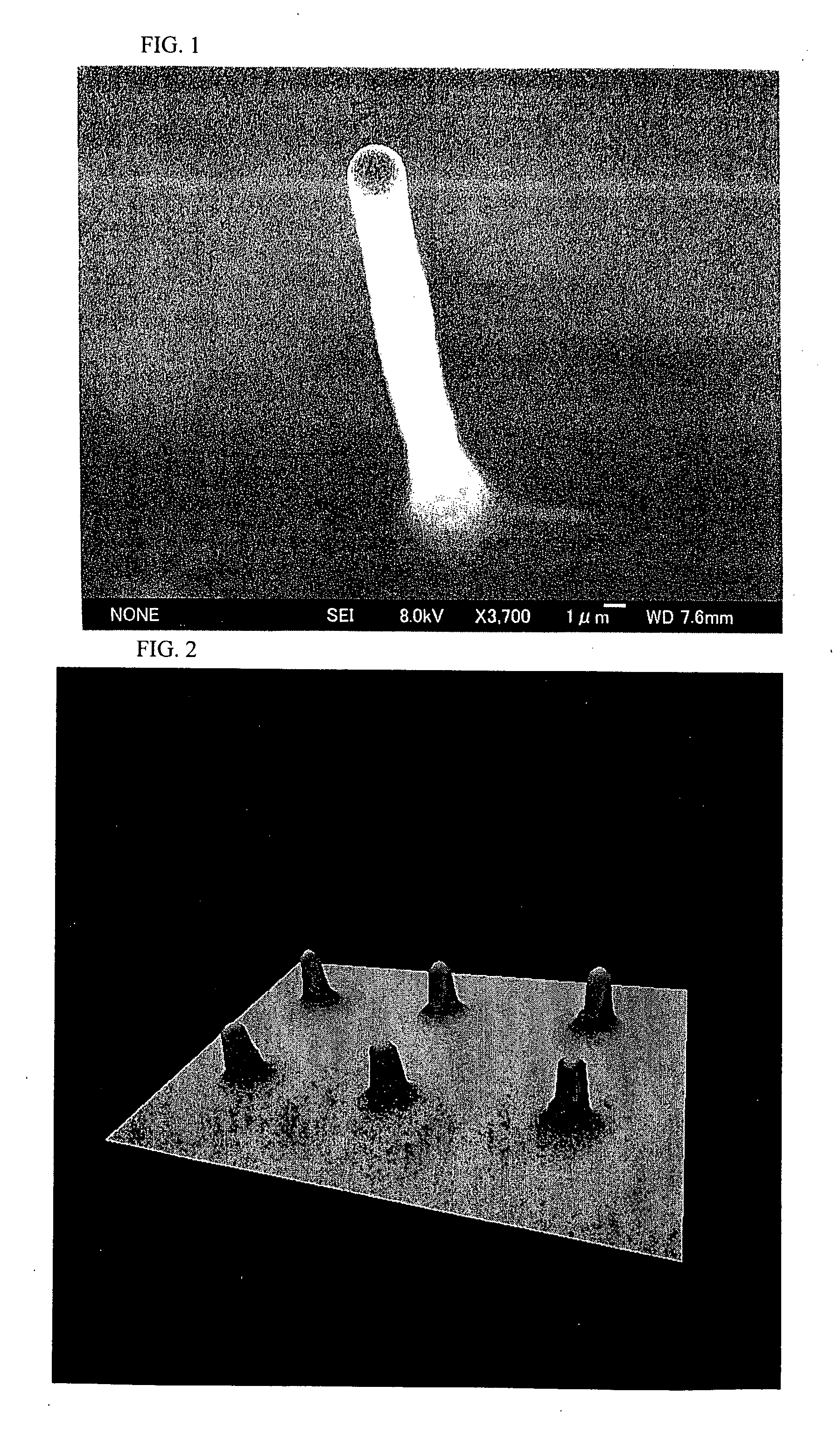
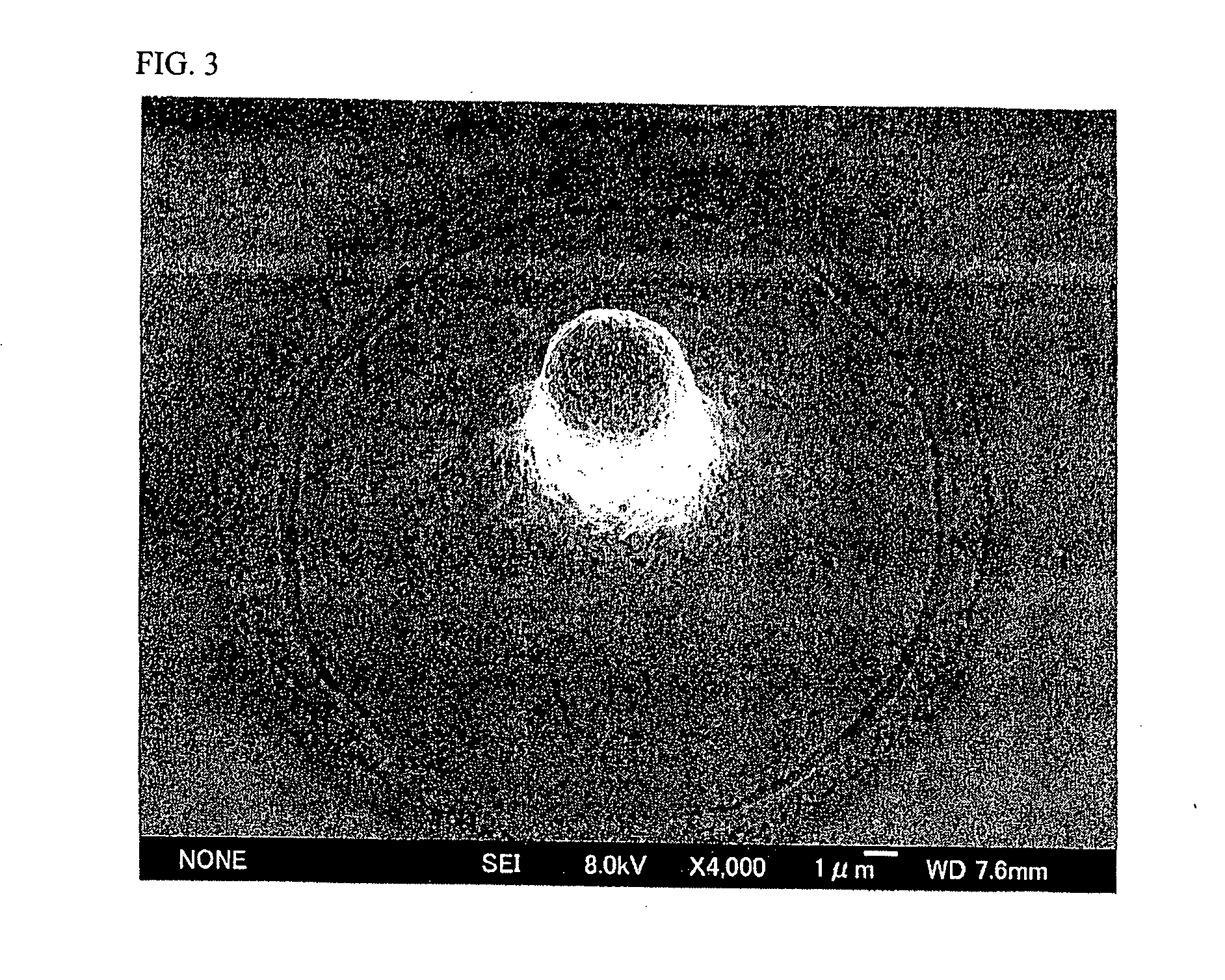
[0156] Using the silver nanoparticle dispersion prepared in Example 1, a disc-like pattern whose base is 4.5 ?m in diameter is formed on glass by an ultrafine-droplet fluid ejecting apparatus (ultrafine inkjet apparatus). The drawing condition was the same as that of Example 1. The coated film thickness per application was 0.3 μm and the dispersion was repeatedly coated to the same pattern several times to prepare a disc-like silver nanoparticle coating layer having a layered thickness of 3.5 μm. After the drawing, the disc-like silver nanoparticle layer on the glass was subjected to heat treatment at 240?C for 1 hour to sinter the silver nanoparticle layer, whereby a silver nanoparticle sintered product layer was formed. Regarding the outer shape of the obtained sintered product layer, the layer is a disc-like (conical socle) sintered metal pad having a circular base 4.5 μm in diameter and a thickness of 2.5 μm. FIG. 3 is a print out of an image of an outer shape of a sintered meta...

example 9

[0157] Through holes 200 μm in diameter extending between the upper layer surface and the back side (lower layer surface) were formed on a multilayer wiring substrate material. The upper layer of the multilayer wiring substrate on which through holes are made had a thickness of 1.6 mm. The diameter / depth ratio, i.e., the aspect ratio of the through hole is set to as high as 1 / 8. On the back side, a lower surface wiring layer is disposed, and the buried electroconductive member provided in the through hole constitutes via hole connection.

[0158] Using the silver nanoparticle dispersion prepared in Example 1, a buried type coating layer of silver nanoparticles is formed in a through hole 200 μm in diameter by an ultrafine-droplet fluid ejecting apparatus (ultrafine inkjet apparatus). The drawing condition was the same as that of Example 1. The coated film thickness per application was 0.3 μm and the dispersion was repeatedly coated to the through hole several times to prepare a silver...


PUM

PropertyMeasurementUnit
particle sizeaaaaaaaaaa
temperatureaaaaaaaaaa
particle sizeaaaaaaaaaa

Abstract

The present invention provides a dispersion usable for forming an electroconductive layer having an extremely fine pattern and a high thickness / minimum width ratio in the cross-section, and which has a high fluidity enabling application of inkjet to draw a fine pattern at high accuracy and contains only metal nanoparticles as a conductive medium. According to the present invention, a metal nanoparticle dispersion suitable to multiple layered coating by jetting in the form of fine droplets is prepared by dispersing metal nanoparticles having an average particle size of 1 to 100 nm in a dispersion solvent having a boiling point of 80° C. or higher in such a manner that the volume percentage of the dispersion solvent is selected in the range of 55 to 80% by volume and the fluid viscosity (20° C.) of the dispersion is chosen in the range of 2 mPa·s to 30 mPa·s, and then when the dispersion is discharged in the form of fine droplets by inkjet method or the like, the dispersion is concentrated by evaporation of the dispersion solvent in the droplets in the course of flight, coming to be a viscous dispersion which can be applicable to multi-layered coating.

Description

TECHNICAL FIELD [0001] The present invention relates to a conductive metal nanoparticle dispersion having high fluidity, a process for preparing the same and a method of using the conductive metal nanoparticle dispersion, and more specifically metal nanoparticle dispersion applicable to formation of a coating layer being thick in thickness relative to its fine surface pattern size on a substrate by means of inkjet printing, and thus usable for forming a sintered product layer of metal nanoparticles having a high aspect ratio, and to a process for forming a sintered product layer of metal nanoparticles in fine shape with a high aspect ratio with use of the same. BACKGROUND ART [0002] Metal plated films have been widely employed for wiring patterns provided on a mounting board as well as pads at the sites for jointing between semiconductor devices and wiring patterns, which are used in assembling of semiconductor devices so far. Along with recent improvement in the technique of drawin...

Claims


Application Information

Patent Timeline
Patent Type & Authority Applications(United States)
IPC IPC(8): B05D1/12C09D5/24C09D17/00H01B1/02H01B1/22H05K3/12
CPCC09D5/24C09D17/006H01B1/02H01B1/22H05K3/125H05K2201/0257H05K2203/013B22F9/00H01B13/00
Inventor ITOH, DAISUKEIZUMITANI, AKIHITOHATA, NORIAKIMATSUBA, YORISHIGEMURATA, KAZUHIROYOKOYAMA, HIROSHI
Owner HARIMA CHEM INC
Why Eureka
Try Eureka