Laser irradiating device, laser irradiating method and manufacturing method of semiconductor device

a laser irradiation and semiconductor technology, applied in the direction of manufacturing tools, instruments, non-linear optics, etc., can solve the problems of difficult uniform irradiation of laser beams, difficult control of the position of large crystal grains, and hardly possible channel forming regions, etc., to achieve efficient forming of crystalline semiconductor films

Inactive Publication Date: 2007-05-03
SEMICON ENERGY LAB CO LTD
View PDF99 Cites 29 Cited by
  • Summary
  • Abstract
  • Description
  • Claims
  • Application Information

AI Technical Summary

Benefits of technology

[0019] Therefore, an object of the present invention is to provide a method and a device for constantly setting the energy distribution of the laser beam on the irradiating face, and irradiating the uniform laser beam to the above entire irradiating face. Another object of the present invention is to provide a laser irradiating method and a l

Problems solved by technology

However, it is hardly possible that the channel forming region is formed of a single crystal semiconductor film without influence of the crystal grain boundary.
However, the above-mentioned energy region is very narrow, and the position where a large crystal grain is obtained can not be controlled.
Even when such a laser beam is used and irradiated to a semiconduc

Method used


Image

  • Laser irradiating device, laser irradiating method and manufacturing method of semiconductor device
  • Laser irradiating device, laser irradiating method and manufacturing method of semiconductor device
  • Laser irradiating device, laser irradiating method and manufacturing method of semiconductor device

Examples


embodiments

Embodiment 1

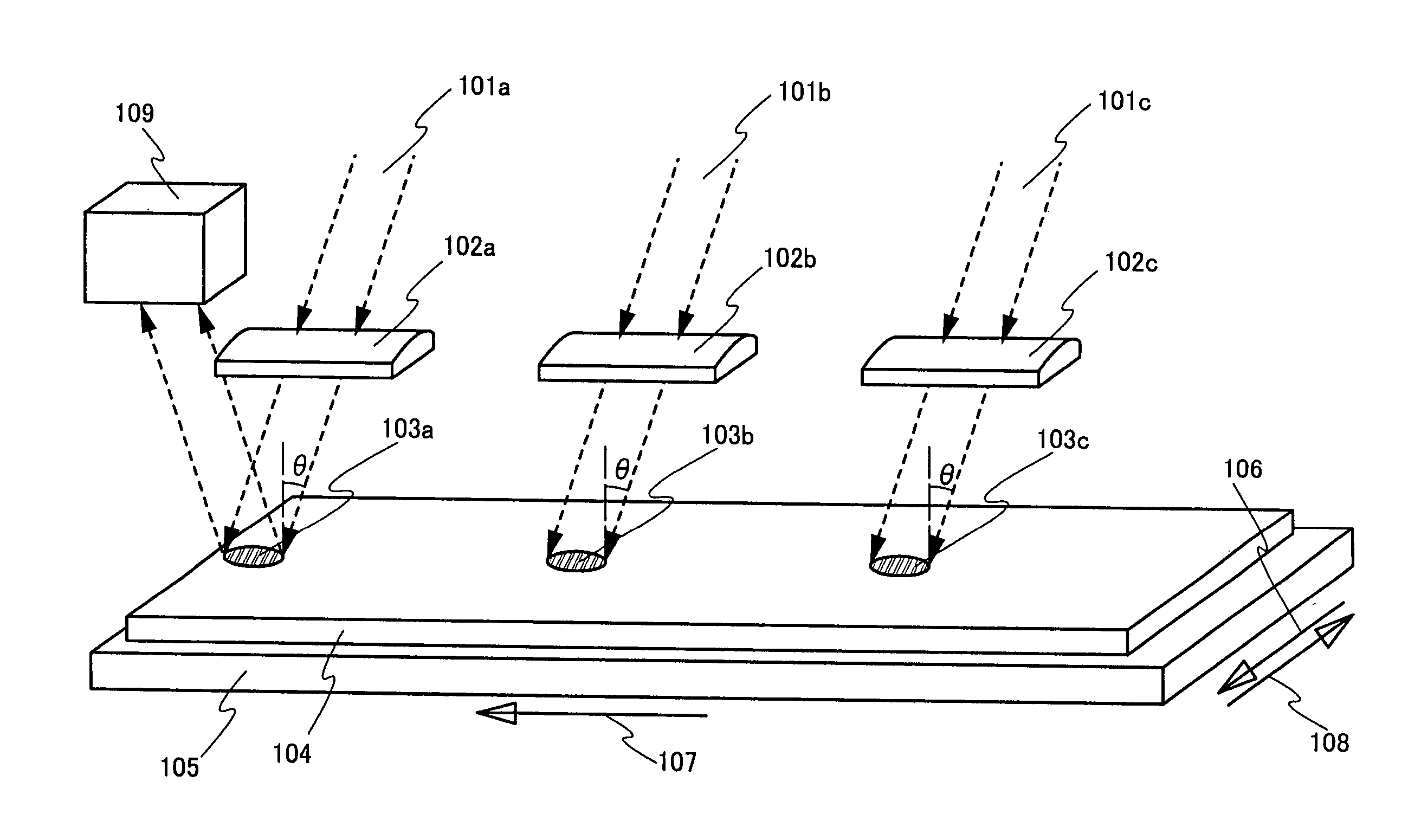
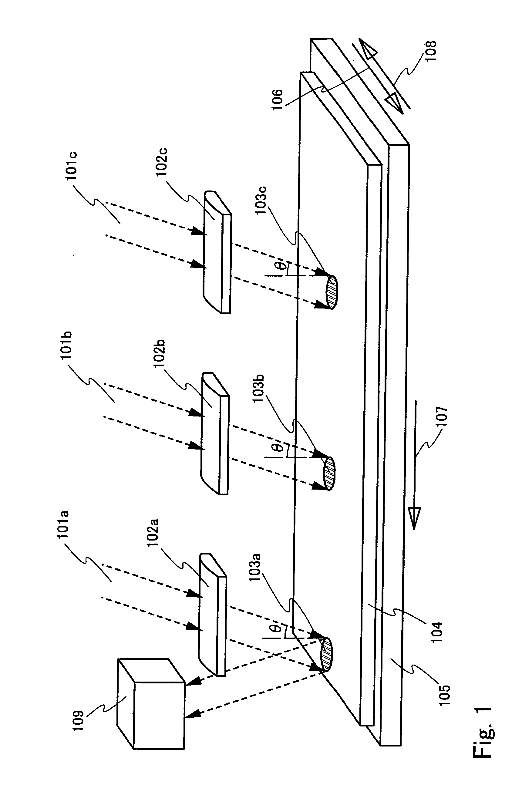
[0072] In this embodiment, a method for slantingly irradiating the plural laser beams to the substrate will be explained by using FIGS. 1, 2A, 2B, 18 and 19.

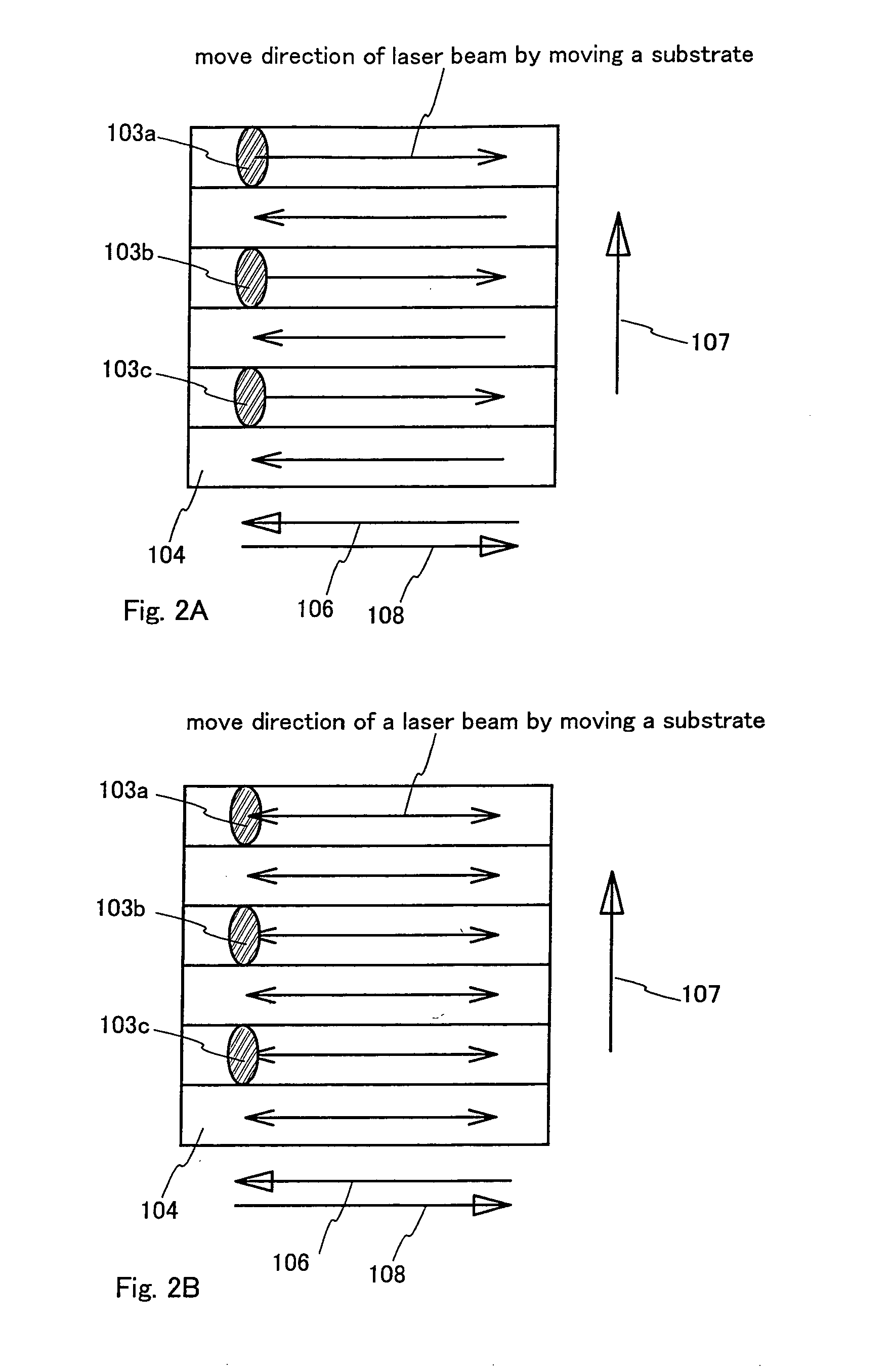
[0073] Each of the plural laser beams 101a, 101b, 101c is shortened in the short side direction by cylindrical lenses 102a, 102b, 102c, and becomes laser beams 103a, 103b, 103c having an elliptical shape or a rectangular shape on an irradiating face. In order to form a laser beam having an elliptical shape or a rectangular shape on an irradiating face, a grating may be used. If a stage (or the substrate) is moved in a direction shown by reference numeral 106, the laser beam can be irradiated in a direction shown by reference numeral 108 without changing the incident angle of the laser beam to the substrate. When the irradiation of the laser beam in the direction shown by reference numeral 108 is terminated, the stage (or the substrate) is moved in a direction shown by reference numeral 107. The laser beam can be ir...

embodiment 2

[0080] In this embodiment, a method for irradiating the plural laser beams from a direction perpendicular to the substrate will be explained by using FIG. 3.

[0081] The laser beams 110a, 110b, 110c oscillated from the laser is shortened by cylindrical lenses 112a, 112b, 112c in the short side direction, and is changed to laser beams 113a, 113b, 113c having an elliptical shape or a rectangular shape on an irradiating face. In order to form a laser beam having an elliptical shape or a rectangular shape on an irradiating face, a grating may be used. If the stage (or the substrate) is moved in a direction shown by reference numeral 106, the laser beam can be irradiated in a direction shown by reference numeral 108 without changing the incident angle of the laser beam to the substrate. When the irradiation of the laser beam in the direction shown by reference numeral 106 is terminated, the stage (or the substrate) is moved in a direction shown by reference numeral 107. The laser beam can...

embodiment 3

[0085] In this embodiment, a method for irradiating the laser beam from the direction perpendicular to the substrate by using plural lasers having the rod shape of a slab type will be explained by using FIG. 4.

[0086] The laser beams 120a, 120b, 120c oscillated from the laser is shortened in the longitudinal direction and the transversal direction by convex lenses 122a, 122b, 122c. This laser beam 120 is converged by cylindrical lenses 123a, 123b, 123c in the longitudinal direction and is then enlarged, and becomes laser beams 124a, 124b, 124c having a rectangular shape on an irradiating face. In order to form a laser beam having an elliptical shape or a rectangular shape on an irradiating face, a grating may be used. If the stage (or the substrate) is moved in a direction shown by reference numeral 106, the laser beam can be irradiated in a direction shown by reference numeral 108 without changing the incident angle of the laser beam to the substrate. When the irradiation of the la...


PUM

PropertyMeasurementUnit
Shapeaaaaaaaaaa
Distributionaaaaaaaaaa

Abstract

An object of the present invention is to provide a method and a device for constantly setting the energy distribution of a laser beam on an irradiating face, and uniformly irradiating the laser beam to the entire irradiating face. Further, another object of the present invention is to provide a manufacturing method of a semiconductor device including this laser irradiating method in a process. Therefore, the present invention is characterized in that the shapes of plural laser beams on the irradiating face are formed by an optical system in an elliptical shape or a rectangular shape, and the plural laser beams are irradiated while the irradiating face is moved in a first direction, and the plural laser beams are irradiated while the irradiating face is moved in a second direction and is moved in a direction reverse to the first direction. The plural laser beams may be irradiated while the irradiating face is moved in the first direction, and the plural laser beams may be irradiated while the irradiating face is moved in the direction reverse to the first direction, and the irradiating face may be also moved in the second direction.

Description

BACKGROUND OF THE INVENTION [0001] The present invention relates to a laser irradiation method of annealing a semiconductor film using a laser beam and a laser irradiation apparatus for performing the laser annealing (apparatus including a laser and an optical system for guiding a laser beam output from the laser to a member to be processed). Further, the present invention relates to a semiconductor device manufactured by the steps including the laser annealing step and a method of manufacturing the semiconductor device. Note that the semiconductor device mentioned through the specification includes an electro-optical device such as a liquid crystal display device or a light emitting device and an electronic device including the electro-optical device as its component. DESCRIPTION OF THE RELATED ART [0002] In recent years, a wide range of researches have been made as to the art of applying laser annealing to a semiconductor film formed on an insulating substrate such as a glass subs...

Claims


Application Information

Patent Timeline
IPC IPC(8): H01L21/20H01S5/06B23K26/067B23K26/073B23K26/10G02F1/1368H01L21/336H01L29/786
CPCB23K26/0656B23K26/067B23K26/0676B23K26/0732B23K26/0736B23K26/10B23K2201/40H01L21/2026H01S3/0071B23K26/066B23K2101/40H01L21/02683H01L21/02422H01L21/02502H01L21/02488H01L21/0242H01L21/02425H01L21/02686H01L21/02678H01L21/02598H01L21/02532H01L21/02381H01L21/02691H01L21/02675
Inventor TANAKA, KOICHIRO
Owner SEMICON ENERGY LAB CO LTD
Why Eureka
Try Eureka