Printed wiring board, its manufacturing method and circuit device

a printing method and wiring board technology, applied in the direction of turning machines, resistive material coating, metallic material coating processes, etc., can solve the problems of warpage deformation of the resulting printed wiring board, troublesome handling of copper film, and it is impossible for the three-layer structure consisting of insulating film, adhesive and copper foil to meet printed wiring boards. , to achieve the effect of high reliability and high insulation resistan

Active Publication Date: 2007-05-10
CHIPBOND TECH
View PDF8 Cites 21 Cited by
  • Summary
  • Abstract
  • Description
  • Claims
  • Application Information

AI Technical Summary

Benefits of technology

[0024] The present invention comprises a step, in which a base metal layer (seed layer or first metal layer) is formed on a surface of an insulating film by sputtering or the like, then a conductive metal such as copper is deposited on a surface of the base metal layer by for example plating, a photoresist is applied to the conductive metal surface and exposed and developed, then using the cured photoresist as a masking material, the copper layer is selectively etched to form a desired wiring pattern, and the base metal layer formed on the insulating film surface is treated with an etching solution capable of dissolving and/or passivating the metal that forms the base metal layer, whereby most of the base metal

Problems solved by technology

If a copper foil having a thickness smaller than this thickness is used, handling of the copper film becomes very troublesome, for example, a copper foil with a support needs to be used.
Further, if a wiring pattern is formed using a copper-clad laminate in which such a thin copper foil is bonded to a surface of an insulating film with an adhesive, warpage deformation of the resulting printed wiring board is brought about by heat shrinkage of the adhesive that is used for bonding the copper foil.
In particular, with miniaturization and lightening of electronic equipments, thinning and lightening of printed

Method used


Image

  • Printed wiring board, its manufacturing method and circuit device
  • Printed wiring board, its manufacturing method and circuit device
  • Printed wiring board, its manufacturing method and circuit device

Examples


example 1

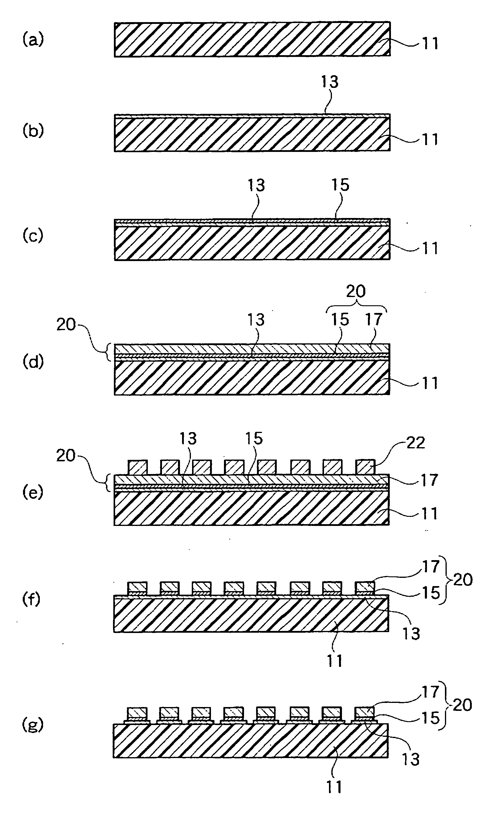
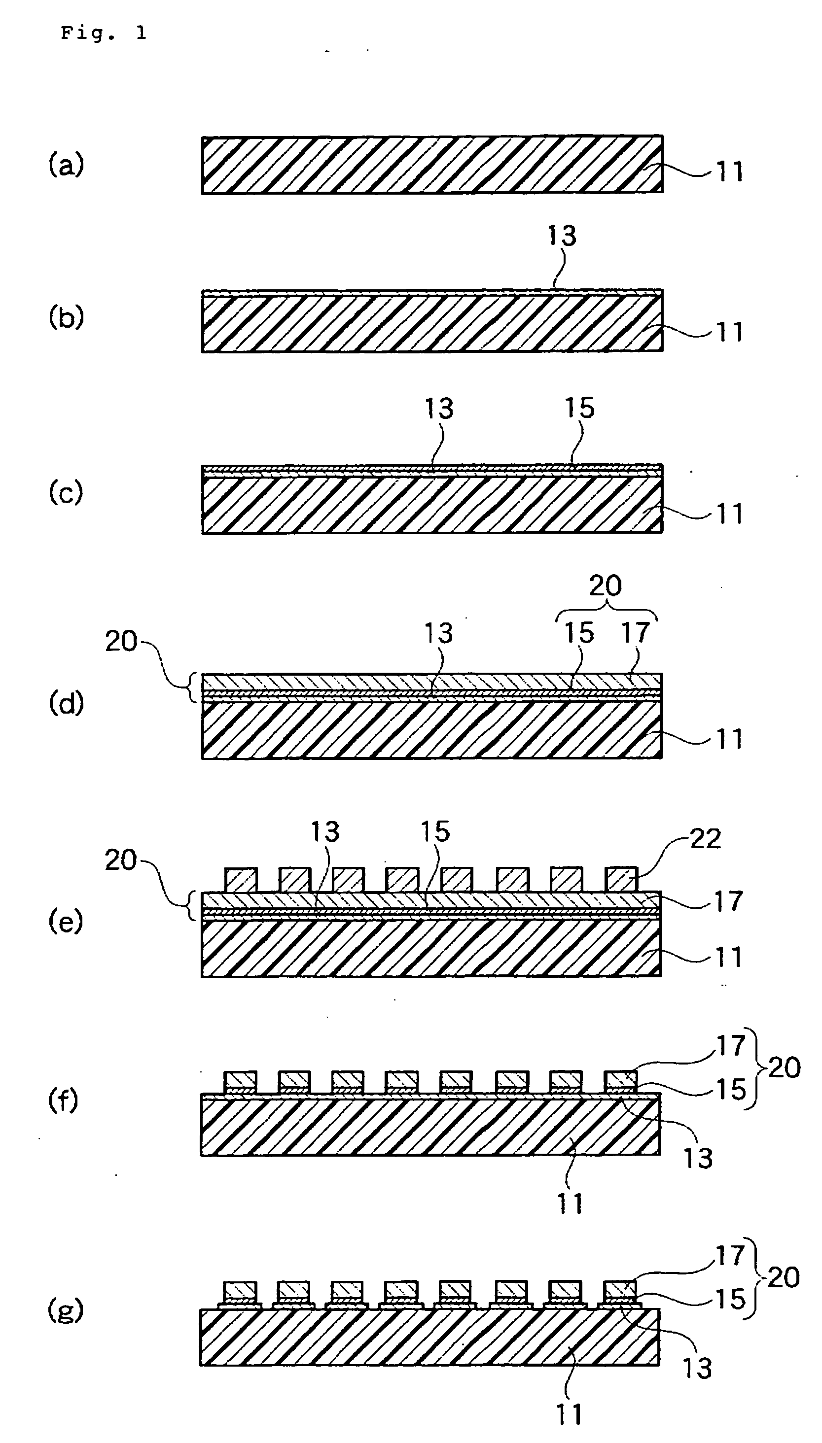
[0075] One surface of a polyimide film having an average thickness of 75 μm (available from Ube Industries, Ltd., Upirex S) was subjected to roughening treatment by back sputtering, and then a nickel-chromium alloy was sputtered under the following conditions to form a chromium-nickel alloy layer having an average thickness of 40 nm as a base metal layer.

[0076] That is to say, the polyimide film of 75 μm thickness was treated at 100° C. and 3×10⁻⁵ Pa for 10 minutes to perform degassing, and then a chromium-nickel alloy was sputtered under the sputtering conditions of 100° C. and 0.5 Pa.

[0077] On the base metal layer formed as above, copper was further sputtered under the conditions of 100° C. and 0.5 Pa to form a sputtering copper layer having an average thickness of 300 nm.

[0078] On the surface of the sputtering copper layer formed as above, copper was deposited by electroplating to form an electrolytic copper layer (electroplating copper layer) having a thickness of 8 μm.

[0079...

example 2

[0084] One surface of a polyimide film having an average thickness of 75 μm (available from Ube Industries, Ltd., Upirex S) was subjected to roughening treatment by back sputtering, and then a nickel-chromium alloy was sputtered under the following conditions to form a chromium-nickel alloy layer having an average thickness of 40 nm as a base metal layer.

[0085] That is to say, the polyimide film of 75 μm thickness was treated at 100° C. and 3×10⁻⁵ Pa for 10 minutes to perform degassing, and then a chromium-nickel alloy was sputtered under the sputtering conditions of 100° C. and 0.5 Pa.

[0086] On the surface of the sputtering base metal layer formed as above, copper was deposited by electroplating to form an electrolytic copper layer (electroplating copper layer) having a thickness of 8 μm.

[0087] The surface of the copper layer (i.e., conductive metal layer) formed as above was coated with a photosensitive resin, and the photosensitive resin was exposed and developed to form a pat...

example 3

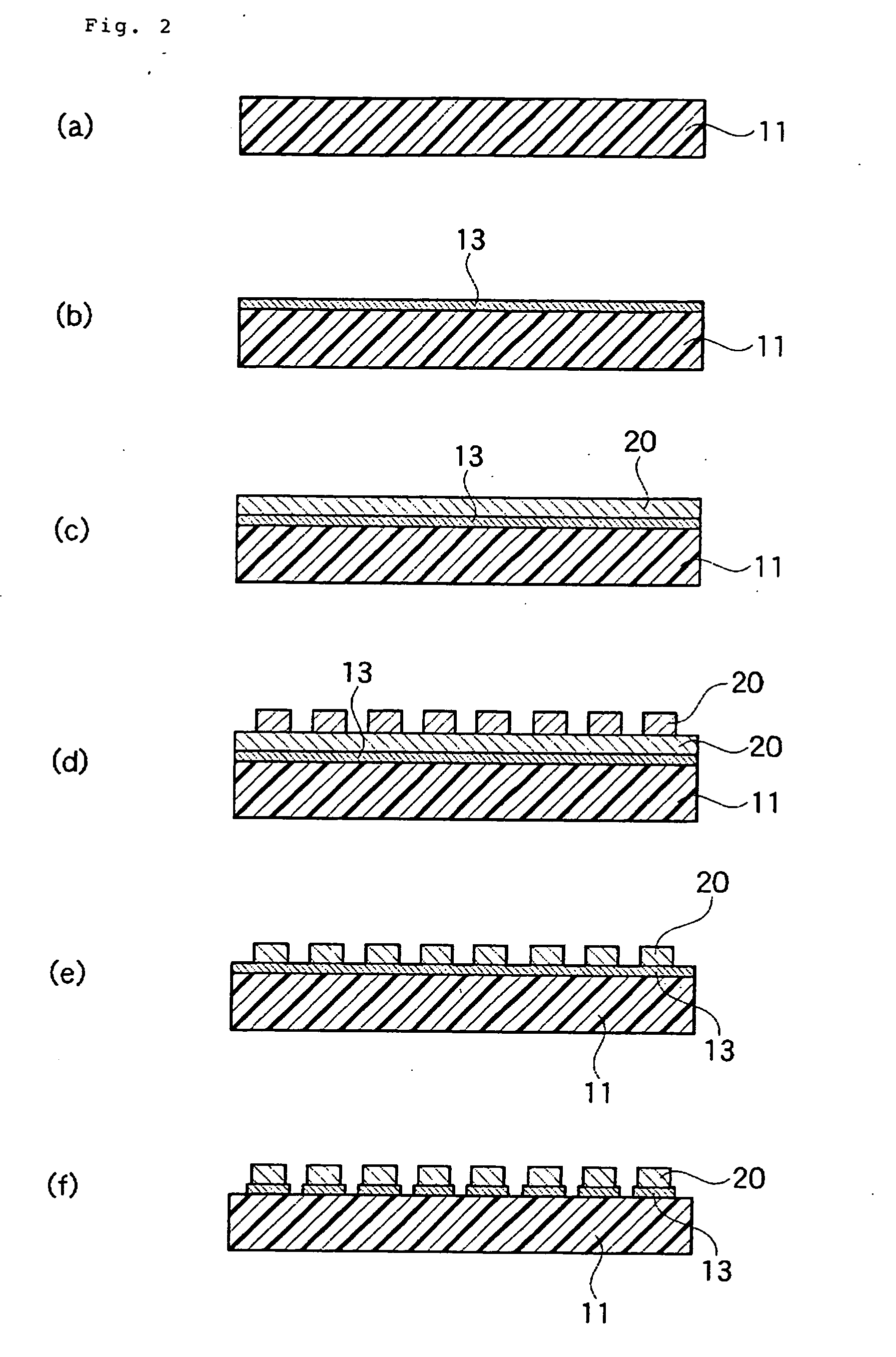
[0094] One surface of a polyimide film having an average thickness of 38 μm (available from Ube Industries, Ltd., Upirex S) was subjected to roughening treatment by back sputtering, and then a nickel-chromium alloy was sputtered in the same manner as in Example 1 to form a chromium-nickel alloy layer having an average thickness of 30 nm as a base metal layer.

[0095] On the base metal layer formed as above, copper was sputtered in the same manner as in Example 1 to form a sputtering copper layer having an average thickness of 200 nm.

[0096] On the surface of the sputtering copper layer formed as above, copper was deposited by electroplating to form an electrolytic copper layer (conductive metal layer) having a thickness of 8 μm.

[0097] The surface of the electrolytic copper layer thus formed was coated with a photosensitive resin, and the photosensitive resin was exposed and developed to form a pattern of a comb-shaped electrode in such a manner that the wiring pitch should become 30...


PUM

PropertyMeasurementUnit
Electrical conductoraaaaaaaaaa
Widthaaaaaaaaaa

Abstract

[Solution means] A process for producing a printed wiring board comprises the steps of depositing a base metal on at least one surface of an insulating film to form a base metal layer and further depositing copper or a copper alloy to form a conductive metal layer, then removing a surface metal layer, which is formed through the above step, by etching to form a wiring pattern, and then treating the base metal layer with a treating liquid capable of dissolving and/or passivating the metal that forms the base metal layer. The printed wiring board so provided comprises an insulating film and a wiring pattern formed on at least one surface of the insulating film, the wiring pattern including a base metal layer deposited on the insulating film surface and a conductive metal layer, the base metal layer for forming the wiring pattern protrudes in a widthwise direction more than the conductive metal layer for forming the wiring pattern.

Description

TECHNICAL FIELD [0001] The present invention relates to a printed wiring board in which a wiring pattern is directly formed on a surface of an insulating film without interposing an adhesive layer, a process for producing the printed wiring board, and a circuit board mounted with an electronic part. More particularly, the present invention relates to a printed wiring board formed from a laminate of a two-layer structure consisting of an insulating film that becomes a substrate and a metal layer formed on a surface of the insulating substrate, a process for producing the printed wiring board, and a circuit device mounted with an electronic part. BACKGROUND ART [0002] Wiring boards have been heretofore produced by the use of copper-clad laminates in which a copper foil is laminated onto a surface of an insulating film such as a polyimide film using an adhesive. [0003] Such a copper-clad laminate is produced by thermally bonding a copper foil under pressure to an insulating film having...

Claims


Application Information

Patent Timeline
IPC IPC(8): H05K3/00H05K3/02H05K3/06H05K3/38
CPCH05K3/06H05K3/388H05K2201/0338Y10T29/5164H05K3/381Y10T29/49155Y10T29/49124H05K2201/098H05K1/02H05K3/18
Inventor KATAOKA, TATSUOAKASHI, YOSHIKAZUIGUCHI, YUTAKA
Owner CHIPBOND TECH
Why Eureka
Try Eureka