Vertical gallium-nitride based light emitting diode

a technology of light emitting diodes and galliumnitride, which is applied in the direction of basic electric elements, electrical equipment, semiconductor devices, etc., can solve the problems of cost-reducing, improving optical power and chip characteristics, and reducing the size of gans, so as to improve the light extraction efficiency, improve the reflectivity of the passivation layer formed of dbr, and improve the effect of light extraction efficiency

Active Publication Date: 2007-05-24
SAMSUNG ELECTRONICS CO LTD
View PDF2 Cites 75 Cited by
  • Summary
  • Abstract
  • Description
  • Claims
  • Application Information

AI Technical Summary

Benefits of technology

[0012] An advantage of the present invention is that it provides a vertical GaN-based LED that can improve the light extraction efficiency. In the vertical GaN-based LED, a passivation layer is formed of a distributed Bragg reflector (DBR) having high reflectivity between a light-emitting structure and a plating seed layer. Therefore, some of light emitted from the light-emitting structure can be prevented from being absorbed or scattered into the plating seed layer.
[0013] Additional aspects and advantages of the present general inventive concept will be set forth in part in the description which follows and, in part, will be obvious from the description, or may be learned by practice of the general inventive concept.
[0014] According to an aspect of the invention, a vertical GaN-based LED includes: an n-electrode; a light-emitting structure in which an n-type GaN layer, an active layer, and a p-type GaN layer are sequentially formed under the n-electrode; a p-electrode formed under the light-emitting structure; a passivation layer formed to cover the side and bottom surfaces of the light-emitting structure and expose a predetermined portion of the p-electrode, the passivation layer being formed of a distributed Bragg reflector (DBR); a plating s

Problems solved by technology

Therefore, it is difficult to reduce the size of the GaN-based LED

Method used


Image

  • Vertical gallium-nitride based light emitting diode
  • Vertical gallium-nitride based light emitting diode
  • Vertical gallium-nitride based light emitting diode

Examples


embodiment 1

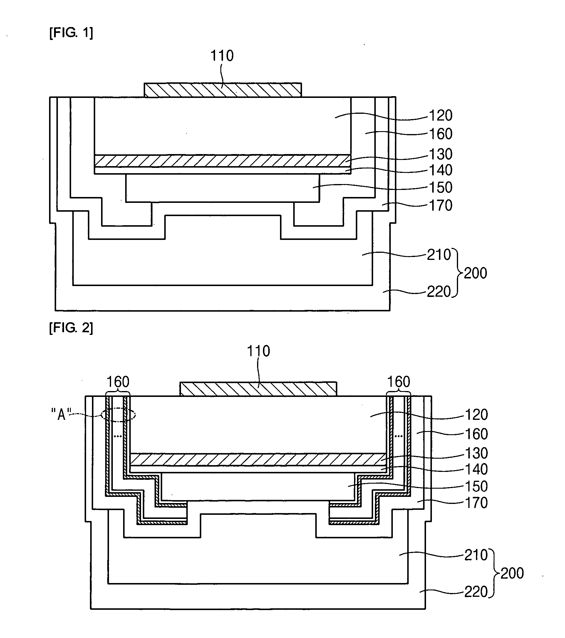
[0027] A vertical GaN-based LED according to a first embodiment of the present invention will be described below with reference to FIGS. 2 and 3.

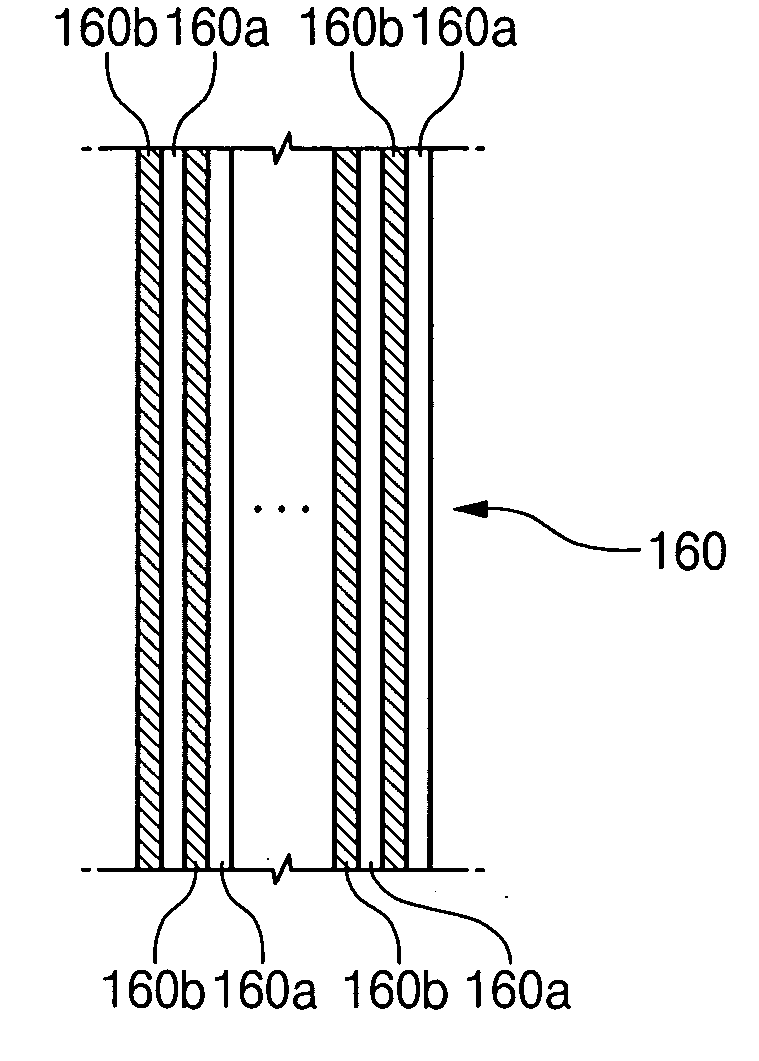
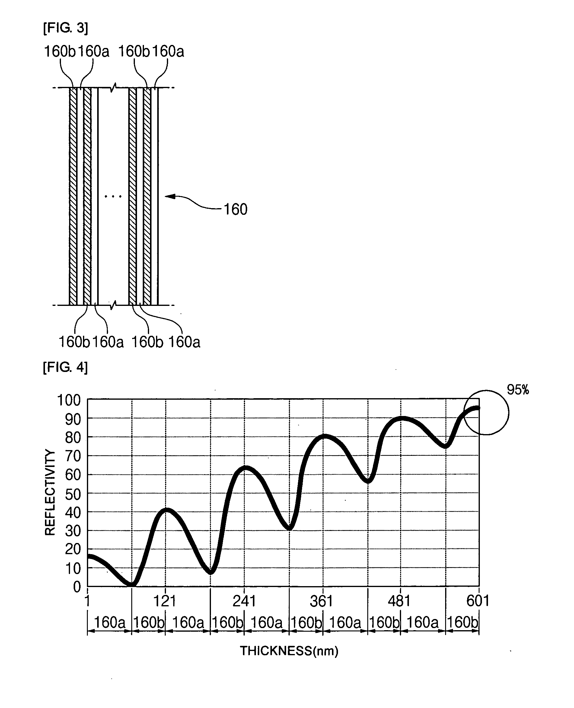
[0028]FIG. 2 is a sectional view of a vertical GaN-based LED according to a first embodiment of the present invention, and FIG. 3 is a partial sectional view of a passivation layer illustrated in FIG. 2.

[0029] Referring to FIGS. 2 and 3, an n-type bonding pad (not shown) for electrical connection to an external device is formed on the uppermost portion of the vertical GaN-based LED.

[0030] An n-electrode 110 is formed under the n-type bonding pad. It is preferable that the n-electrode 110 is formed of metal having high reflectivity so that it can serve as an electrode and a reflective layer.

[0031] An n-type GaN layer 120 is formed under the n-electrode 110. More specifically, the n-type GaN layer 120 may be formed of an n-doped GaN layer or an n-doped GaN / AIGaN layer.

[0032] To improve the current spreading efficiency, an n-type transpar...

embodiment 2

[0045] A vertical GaN-based LED according to a second embodiment of the present invention will be described below with reference to FIG. 6. Description about the same parts as the first embodiment of the present invention will be omitted.

[0046]FIG. 6 is a sectional view of a vertical GaN-based LED according to a second embodiment of the present invention.

[0047] Referring to FIG. 6, the vertical GaN-based LED according to the second embodiment of the present invention is similar to the vertical GaN-based LED according to the first embodiment of the present invention, but is different in that a plating seed layer 170 is composed of a bi-layer in which an adhesive layer 170a and a reflective layer 170b are sequentially formed, not a single layer formed of metal such as Au, Cu, Ta, and Ni.

[0048] The adhesive layer 170a of the plating seed layer 170 is formed of metal having excellent adhesive property with respect to oxide materials. That is, the adhesive layer 170a is formed of meta...


PUM


Abstract

A vertical GaN-based LED includes: an n-electrode; a light-emitting structure in which an n-type GaN layer, an active layer, and a p-type GaN layer are sequentially formed under the n-electrode; a p-electrode formed under the light-emitting structure; a passivation layer formed to cover the side and bottom surfaces of the light-emitting structure and expose a predetermined portion of the p-electrode, the passivation layer being formed of a distributed Bragg reflector (DBR); a plating seed layer formed under the passivation layer and the p-electrode; and a support layer formed under the plating seed layer.

Description

CROSS-REFERENCE TO RELATED APPLICATIONS [0001] This application claims the benefit of Korean Patent Application No. 2005-112162 filed with the Korean Industrial Property Office on Nov. 23, 2005, the disclosure of which is incorporated herein by reference. BACKGROUND OF THE INVENTION [0002] 1. Field of the Invention [0003] The present invention relates to a vertical gallium-nitride (GaN)-based light emitting diode (LED), and more particularly, to a vertical GaN-based LED in which light emitted to a side surface of the vertical GaN-based LED is reflected toward an emission surface, thereby implementing high brightness. [0004] 2. Description of the Related Art [0005] Generally, GaN-based LEDs are grown on a sapphire substrate. The sapphire substrate is rigid and electrically nonconductive and has a low thermal conductivity. Therefore, it is difficult to reduce the size of the GaN-based LED for cost-down or improve the optical power and chip characteristics. Particularly, heat dissipati...

Claims


Application Information

Patent Timeline
IPC IPC(8): H01L33/00H01L33/06H01L33/10H01L33/32
CPCH01L33/0079H01L33/46H01L33/385H01L33/0093
Inventor JANG, TAE SUNGLEE, SU YEOLCHOI, SEOK BEOM
Owner SAMSUNG ELECTRONICS CO LTD
Why Eureka
Try Eureka