

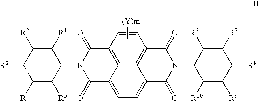
N,N'-dicycloalkyl-substituted naphthalene-based tetracarboxylic diimide compounds as n-type semiconductor materials for thin film transistors
a technology of tetracarboxylic diimide and n-type semiconductors, which is applied in the direction of naphthalimide/phthalimide dyes, synthetic resin layered products, nanoinformatics, etc., can solve the problems of amorphous silicon still having its drawbacks, amorphous silicon still has its drawbacks,
- Summary
- Abstract
- Description
- Claims
- Application Information
AI Technical Summary
Benefits of technology
Problems solved by technology
Method used
Image

Examples
example 2
[0085] This example demonstrates the improved performance of an n-type TFT device using N,N′-dicyclohexyl-1,4,5,8-naphthalene tetracarboxylic acid diimide (Compound I-3) in accordance with the present invention.
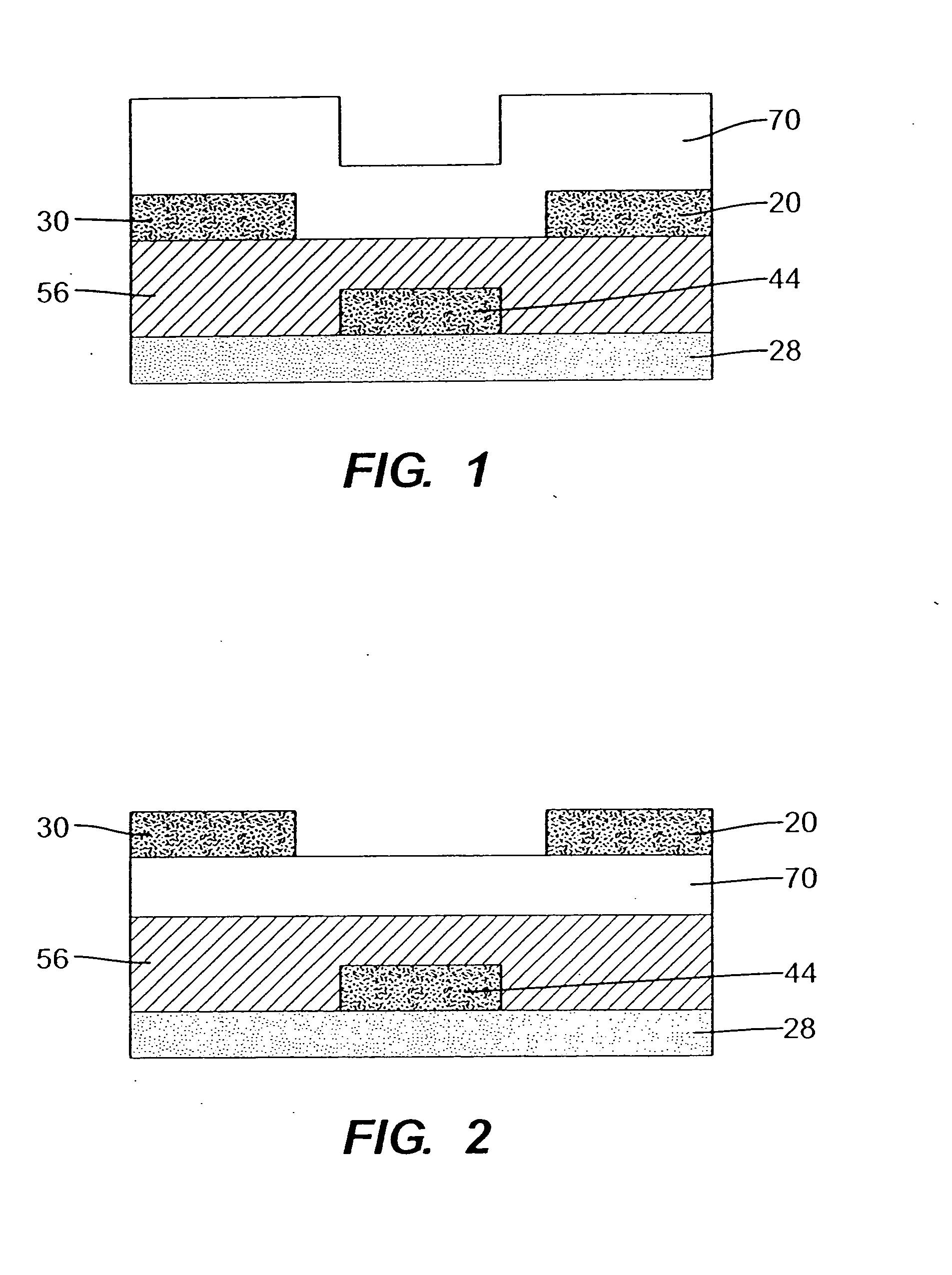
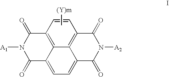
[0086] An n-type TFT device comprising Compound I-3 as the active material was made as in Comparative Example 1. Accordingly, Compound I-3 was deposited by vacuum sublimation at a pressure of 2×10⁻⁷ Torr and a rate of 0.5 Angstroms per second to a thickness of 25 nm as measured by a quartz crystal. During deposition the substrate was held at a constant temperature of 90° C. The sample was exposed to air for a short time prior to subsequent deposition of Au source and drain electrodes through a shadow mask to a thickness of 50 nm. The devices made had an approximately 420 micron channel width, with channel lengths varying from 50 to 175 microns. Multiple organic thin film transistors (OTFTs) were prepared and representative sample of 4 to 12 OTFTs were tested for each deposit...
PUM
| Property | Measurement | Unit |
|---|---|---|
| Temperature | aaaaa | aaaaa |
| Area | aaaaa | aaaaa |
| Area | aaaaa | aaaaa |
Abstract
Description
Claims
Application Information