Maintenance of photoresist activity on the surface of dielectric arcs for 90 nm feature sizes

a dielectric arc and feature size technology, applied in the field of maintenance, can solve the problems of increasing the maintenance cost of the chamber in terms of throughput, increasing and increasing the cost of carbon particulate byproducts of the deposition process, so as to reduce the foot print of the photoresist, the feature size is smaller, and the force exerted on the photoresist wall.

Inactive Publication Date: 2007-05-24
APPLIED MATERIALS INC
View PDF6 Cites 2 Cited by
  • Summary
  • Abstract
  • Description
  • Claims
  • Application Information

AI Technical Summary

Benefits of technology

[0018] We have traced the detachment of photoresist during development of patterned features in the range of about 90 nm and smaller to a combination of the reduced “foot print” of the pattern on the underlying substrate and to the contact angle between the underlying substrate surface and the developing reagent used to develop a pattern in the photoresist. We have determined that by maintaining a contact angle of about 20 degrees or greater, and preferably 35 degrees or greater, the detachment of the photoresist from the underlying substrate can be avoided for photoresists including feature sizes in the range of about 90 nm. As feature sizes grow even smaller, it may be necessary to continually increase the contact angle to maintain adhesion of the photoresist to the underlying substrate during development of the photoresist. The key is to reduce the force exerted against the photoresist wall as the feature size becomes smaller, with the concurrent reduction in foot print of the photoresist on the underlying substrate surface.
[0019] The contact or wetting angle of the substrate depends on the composition of both the substrate and the developer used for photoresist development. The embodiments described below pertain to a DARC, and in particular a DARC comprised of SiOxHy: C, where x ranges from greater than 1 to about 2.0, and H ranges from about 0.1 to about 0.3, and the carbon content ranges from 0% up to 5.0% (typically less than about 3.0%). The reagents used to produce the DARC by PECVD are typically SiH4, and CO2, with helium added as a diluent plasma source gas, which also provides species for surface bombardment of the depositing film. For a silane-based PECVD film deposition process, where the silicon-containing precursor is SiH4, the carbon content in the polymeric film structure is typically less than about 3%, which is contributed by CO2 used in the firm formation process. We have discovered that an increase in carbon content of the DARC produces a higher contact angle, which is beneficial in terms of reducing the potential for detachment of the photoresist from the DARC surface during development of the photoresist using a water based developer of the kind commonly used in the semiconductor industry. To achieve a higher carbon content in the DARC, the amount of CO2 used in the SiH4 / CO2 process may be increased to some extent; in an alternative, the silane-based precursor used in the PECVD deposition of the DARC may contain carbon, such as trimethyl silane ((CH3)3HSi) or tetramethyl silane ((CH3)4 Si), for example, but not by way of limitation.
[0020] Other Group IV elements such as silicon, germanium, tin and lead, by way of example and not by way of limitation, which are present in the DARC film may be increased in concentration, in a manner similar to the carbon content, to increase the contact angle between the DARC surface and the fluid photoresist developer.
[0021] While an increased carbon content in the DARC increases the contact angle and has a beneficial effect in terms of reducing photoresist detachment from the DARC surface during development, a higher carbon content in a silane precursor for PECVD film formation is generally more expensive and carbon particulate byproducts of the film deposition may require more frequent deposition process chamber cleaning. The improved attachment of the photoresist during development may justify the increased chamber maintenance costs in terms of throughput in some instances. As an alternative, it is possible to use a lower carbon content DARC, but to use a surface treatment of the DARC to increase the contact angle with the developer; or to use a developer which provides a higher contact angle on the DARC surface.
[0022] We have achieved an increased contact angle between the DARC surface and a water-based, basic CAR photoresist developer by treating the surface of the DARC after formation of the DARC film. In particular, the DARC film surface has been treated with a hydrogen plasma or a helium plasma to provide an increase in the contact angle. Preferably, the hydrogen plasma is used for the DARC film surface treatment, as this process provides a greater shelf life for the DARC coated substrate prior to subsequent use and provides very good uniformity of performance across the entire substrate.
[0023] The most commonly used DUV photoresists for semiconductor device manufacture are the positive chemically amplified photoresists (CARs), which rely upon the generation of an acid in the irradiated portion of the photoresist to form a latent image which is subsequently developed using a basic developer. The photoresist pattern developer is commonly a basic, water-based developer. The presence of a base on the surface of a DARC at the time the CAR is applied causes subsequent problems in pattern production, because the acid generated in the CAR upon irradiation reacts with the base on the surface of the DARC, producing areas at the interface of the DARC and the CAR which do not contain the acid generated by the irradiation. Development of the photoresist pattern at this interfacial area does not occur properly when the basic developing agent is applied to the photoresist. We have discovered that it is not enough to remove nitrogen-containing species from the surface of the DARC. It is also necessary to reduce the presence of OH groups from the surface of the DARC. The treatment of the DARC surface with a hydrogen plasma prior to photoresist application to the DARC surface not only increases the contact angle between the DARC and a water-based photoresist developer, it also reduces the available OH groups on the surface of the DARC, reducing photoresist poisoning during deposition, and pattern latent image formation of the photoresist. Treatment of the DARC surface with helium prior to photoresist application also tends to reduce the available OH groups on the surface of the DARC, but has a limited performance time window, and has been less uniform in ability to reduce photoresist poisoning under currently known treatment conditions.

Problems solved by technology

While an increased carbon content in the DARC increases the contact angle and has a beneficial effect in terms of reducing photoresist detachment from the DARC surface during development, a higher carbon content in a silane precursor for PECVD film formation is generally more expensive and carbon particulate byproducts of the film deposition may require more frequent deposition process chamber cleaning.
The improved attachment of the photoresist during development may justify the increased chamber maintenance costs in terms of throughput in some instances.

Method used


Image

  • Maintenance of photoresist activity on the surface of dielectric arcs for 90 nm feature sizes
  • Maintenance of photoresist activity on the surface of dielectric arcs for 90 nm feature sizes
  • Maintenance of photoresist activity on the surface of dielectric arcs for 90 nm feature sizes

Examples


example embodiments

Example One

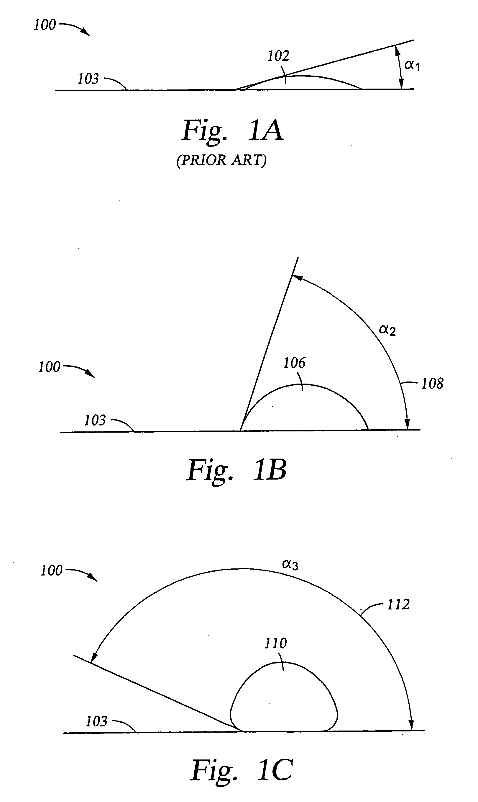
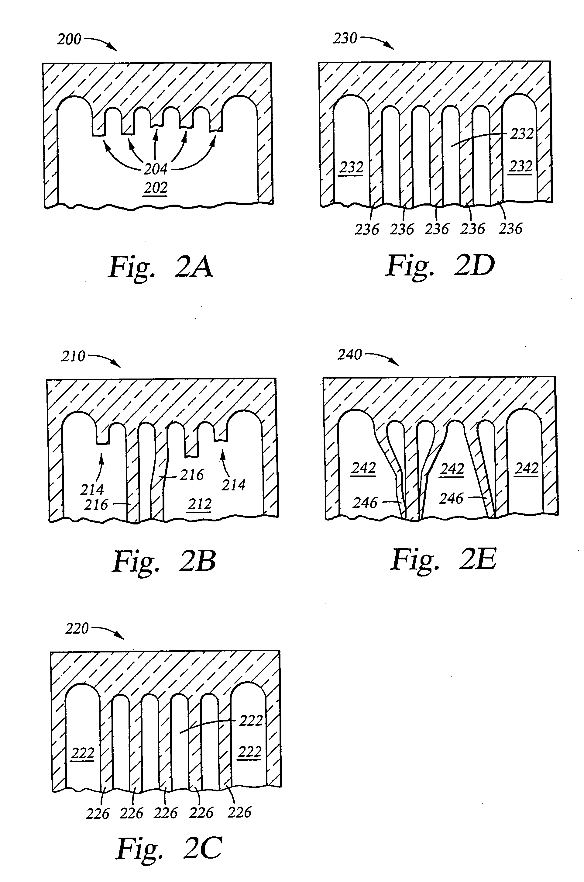
[0063] As a comparative example, a SiON DARC having an n (refractive index) of 1.9 and a k (extinction coefficient)of 0.3@248 nm was capped with a 50 Å thick silicon oxide capping film generated from a SiH4 / CO2 / helium plasma using the general PECVD conditions of the kind described above for a single frequency plasma deposition process. The capped DARC exhibited a contact angle of 5.1 degrees with the water based alkaline developer used to develop the CAR, which was the SHIPLEY® UV6 photoresist. After exposure to either 230 J or 280 J of 248 nm patterning radiation, followed by development of the pattern, a photomicrograph of a top view 200 of the developed photoresist had the appearance illustrated by the schematic shown in FIG. 2A. The oxide-capped SiON DARC surface 202 was completely exposed in patterned areas after development of the photoresist, because the lines and spaces pattern which was to be developed failed due to detachment of the photoresist during developme...

example two

[0064] As a second comparative example, a nitrogen-free DARC 193 SiOxHy: C film having an n of 1.9 and a k of 0.3@248 nm, which was surface treated with a CO2 plasma for a time period of about 20 seconds, using a CO2 flow rate of about 3slm in a 200 mm PRODUCER® twin PECVD process chamber, using the single frequency plasma ! deposition process. The pressure was about 5 Torr, at a substrate temperature of about 350° C., at a plasma source power of about 50-100 W at 13.56 MHz, and at a shower head spacing of 450 mils from the substrate surface. The CO2-treated DARC 193, exhibited a contact angle of only 3.5 degrees with respect to the photoresist water-based alkaline developer. Exposure of the CAR to either 230 J or 280 J of 248 nm patterning radiation, and development of the imaged photoresist resulted in a developed photoresist where none of the patterned areas were present. All of the developed feature areas became detached from the DARC surface and washed away on development.

example three

[0065] As a third comparative example, a nitrogen-free DARC 193 SiOxHy: C film having an n of 1.9 and a k of 0.3@248 nm, which was not surface treated, exhibited a contact angle of about 3.7 degrees with respect to the same developer mentioned with respect to Example Two. Exposure of the SHIPLEY® UV6 photoresist to 230 J of 248 nm patterning radiation, followed by development of the latent irradiated image in the photoresist, produced a relatively acceptable pattern. However, exposure of the CAR to 280 J of 248 nm patterning radiation, followed by development, produced a defective pattern in the CAR of the kind illustrated in FIG. 2B. FIG. 2B is a schematic top view 210 of a photomicrograph of the patterned photoresist. The DARC 193 surface 212 was exposed in some areas where the photoresist 216 should have been present. The photoresist 216 became detached, leaving broken off areas 214 where photoresist was missing. The difference in the developed pattern with such a slight differen...


PUM

PropertyMeasurementUnit
feature sizesaaaaaaaaaa
sizesaaaaaaaaaa
sizesaaaaaaaaaa

Abstract

We have determined that it is necessary to remove hydroxyl groups from the surface of a DARC over which a CAR photoresist is applied, to reduce poisoning of the photoresist during imaging. The poisoning is reduced by treating the surface of the DARC film with a hydrogen or helium-containing plasma which is capable of removing the hydroxyl groups.

Description

[0001] The present application is a continuation application of U.S. application Ser. No. 10 / 724,454, which was filed Nov. 28, 2003, and which is currently pending.BACKGROUND OF THE INVENTION [0002] 1. Field of the Invention [0003] The present invention relates to the fabrication of semiconductor devices having feature sizes in the range of 90 nm and smaller. In particular, the invention relates to a method of maintaining the adhesion of a photoresist to a surface during development of a pattern in the photoresist and to maintenance of the functionality of a chemically amplified photoresist on the surface of a dielectric anti-reflection coating (DARC). [0004] 2. Description of the Background Art [0005] As semiconductor devices are becoming ever smaller, the device features necessarily become smaller. To produce feature sizes in the range of about 124 nm, for example, a chemically amplified photoresist (CAR) is pattern imaged using a DUV wavelength in the range of about 248 nm. To pr...

Claims


Application Information

Patent Timeline
Patent Type & Authority Applications(United States)
IPC IPC(8): G03C5/00G03C5/18G03F7/09G03F7/16G03F7/32
CPCG03F7/091G03F7/16G03F7/322
Inventor AHN, SANG H.RATHI, SUDHABOTHELHO, HERALDO L.
Owner APPLIED MATERIALS INC
Why Eureka
Try Eureka