Semiconductor device having group III nitride buffer layer and growth layers

a semiconductor and nitride technology, applied in the direction of polycrystalline material growth, crystal growth process, chemically reactive gas growth, etc., can solve the problems of film p-type doping, film is unintentionally doped with nitrogen vacancies during growth, and hampered developmen

Inactive Publication Date: 2007-05-31
TRUSTEES OF BOSTON UNIV
View PDF99 Cites 10 Cited by
  • Summary
  • Abstract
  • Description
  • Claims
  • Application Information

AI Technical Summary

Problems solved by technology

Despite the desirability of a mono-crystalline GaN layer, its development has been hampered by the many problems encountered during the growth process.
Hence, the film is unintentionally doped with nitrogen vacancies during growth.
Efforts to dope the film p-type were not successful.

Method used


Image

  • Semiconductor device having group III nitride buffer layer and growth layers
  • Semiconductor device having group III nitride buffer layer and growth layers
  • Semiconductor device having group III nitride buffer layer and growth layers

Examples


example 1

[0078] One example of a light emitting diode having a p-n junction according to the present invention is described below. This example is not intended to limit the invention.

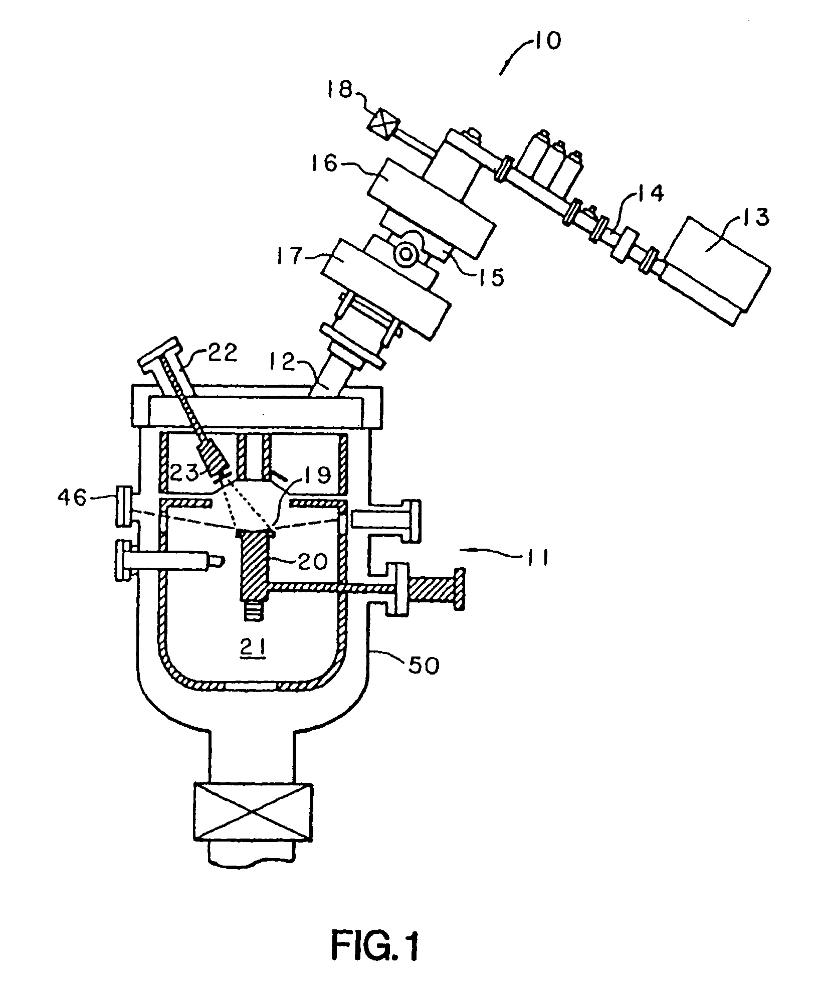
[0079] A (001) sapphire substrate was first subjected to a nitridation process at 850° C. to convert its surface to atomically smooth AlN. Next, a GaN-buffer approximately 300 Å thick was deposited at about 500° C. Following the deposition of the GaN-buffer, the substage was heated to about 800° C. and an autodoped n-type GaN film approximately 2 μm was deposited at a deposition rate of 0.2 μ / hr. Then, a Mg-doped p-layer approximately 0.5 μm thick was deposited by incorporating Mg which was sublimated from a conventional Knudsen cell at 230° C. The Mg flux was then gradually raised by about an order of magnitude by increasing the cell temperature to about 270° C. near the end of the run to facilitate the electrical contacting of the top p-layer. The device was grown with a reduced diameter aperture of about 1 c...

example 2

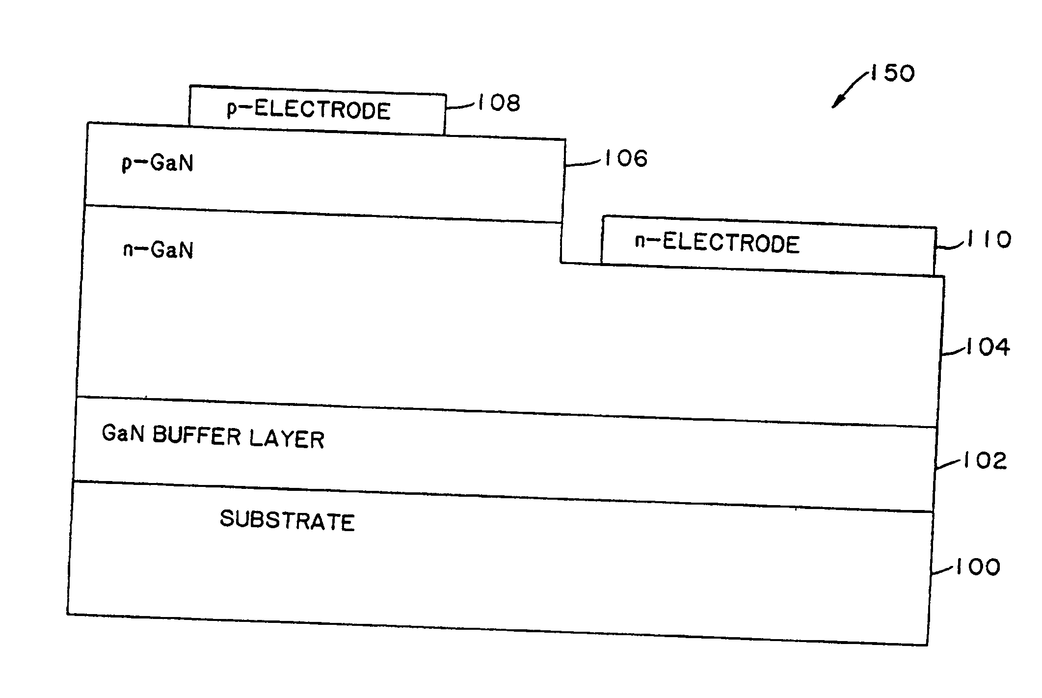
[0086] An LED device was grown using a procedure as set out in Example 1 with an external solenoid. Instead of placing the contacts on the p-type layer, reactive ion etching was performed to expose the underlying n-type layer. A p-electrode and an n-electrode were then formed on the p-type layer and the n-type layer, respectively, followed by rapid thermal annealing of the metal contacts as described above.

Results

[0087] The I-V characteristics of a device as described in Example 2 are illustrated in FIG. 16. The device of Example 2 exhibits excellent I-V characteristics with a turn on voltage of about 3 volts.


PUM

PropertyMeasurementUnit
temperatureaaaaaaaaaa

Abstract

An epitaxial growth system comprises a housing around an epitaxial growth chamber. A substrate support is located within the growth chamber. A gallium source introduces gallium into the growth chamber and directs the gallium towards the substrate. An activated nitrogen source introduces activated nitrogen into the growth chamber and directs the activated nitrogen towards the substrate. The activated nitrogen comprises ionic nitrogen species and atomic nitrogen species. An external magnet and / or an exit aperture control the amount of atomic nitrogen species and ionic nitrogen species reaching the substrate.

Description

CROSS REFERENCE TO RELATED APPLICATIONS [0001] This application is a continuation of application Ser. No. 10 / 610,331 filed Jun. 30, 2003, which is a divisional of application Ser. No. 08 / 560,494 filed Nov. 17, 1995 (now abandoned), which is a divisional of application Ser. No. 08 / 371,708 filed Jan. 13, 1995 (now U.S. Pat. No. 5,633,192), which is a continuation-in-part of application Ser. No. 08 / 113,964 filed Aug. 30, 1993 (now U.S. Pat. No. 5,385,862), which is a continuation of application Ser. No. 07 / 670,692 filed Mar. 18, 1991 (now abandoned), the contents of each are hereby incorporated by reference herein.BACKGROUND OF THE INVENTION [0002] The invention relates to light emitting devices, and specifically to light emitting III-V nitride devices. [0003] Efforts have been made to prepare mono-crystalline GaN because of its potentially useful electrical and optical properties. GaN is a potential source of inexpensive and compact solid-state blue lasers. The band gap for GaN is app...

Claims


Application Information

Patent Timeline
Patent Type & Authority Applications(United States)
IPC IPC(8): H01L33/00H01L29/24C30B23/02H01L21/203H01L33/16H01L33/32
CPCC30B23/02C30B25/14C30B29/40C30B29/403C30B29/406C30B30/04H01L21/0237H01L21/0242H01L21/02458H01L21/02513H01L21/0254H01L21/02573H01L21/02631H01L33/007H01L33/16H01L33/32H01L33/325H01L21/02381H01L21/02433C30B23/002H01L21/02579
Inventor MOUSTAKAS, THEODORE
Owner TRUSTEES OF BOSTON UNIV
Why Eureka
Try Eureka