Engineered barrier layer and gate gap for transistors with negative differential resistance

a technology of negative differential resistance and gate gap, which is applied in the field of metal-insulator-emiconductor devices, can solve the problems of difficult accuracy control of charge trap distribution, inaccurate control of pvr, ndr voltage, and/or ndr switching speed values of ndr transistors, etc., and achieve accurate control, accurate control, and/or optimized device characteristics

Inactive Publication Date: 2007-05-31
SYNOPSYS INC
View PDF5 Cites 5 Cited by
  • Summary
  • Abstract
  • Description
  • Claims
  • Application Information

AI Technical Summary

Benefits of technology

[0013] In a negative differential resistance (NDR) transistor, it is desirable to be able to optimize the device characteristics, such as peak-to-valley ratio (PVR), NDR voltage, for different applications / technologies. In conventional NDR transistors, these characteristics are controlled by the distribution of charge traps at the gate dielectric / channel region interface. However, in certain circumstances, accurately controlling the charge trap distribution, and hence, accurately controlling the PVR, NDR voltage, and / or NDR switching speed values for the NDR transistor, can be difficult. By replacing the charge traps with a barrier layer and a charge storage node (layer) in the gate dielectric, greater manufacturing flexibility and improved control over NDR transistor characteristics can be achieved. As a separate approach, by introducing a gap between the source-channel junction and the gate, the electric field within that gap can be significantly enhanced, thereby reducing the NDR voltage. improving the PVR, and increasing the NDR switching speed of the NDR transistor.

Problems solved by technology

However, in certain circumstances, accurately controlling the charge trap distribution, and hence, accurately controlling the PVR, NDR voltage, and / or NDR switching speed values for the NDR transistor, can be difficult.

Method used


Image

  • Engineered barrier layer and gate gap for transistors with negative differential resistance
  • Engineered barrier layer and gate gap for transistors with negative differential resistance
  • Engineered barrier layer and gate gap for transistors with negative differential resistance

Examples


Embodiment Construction

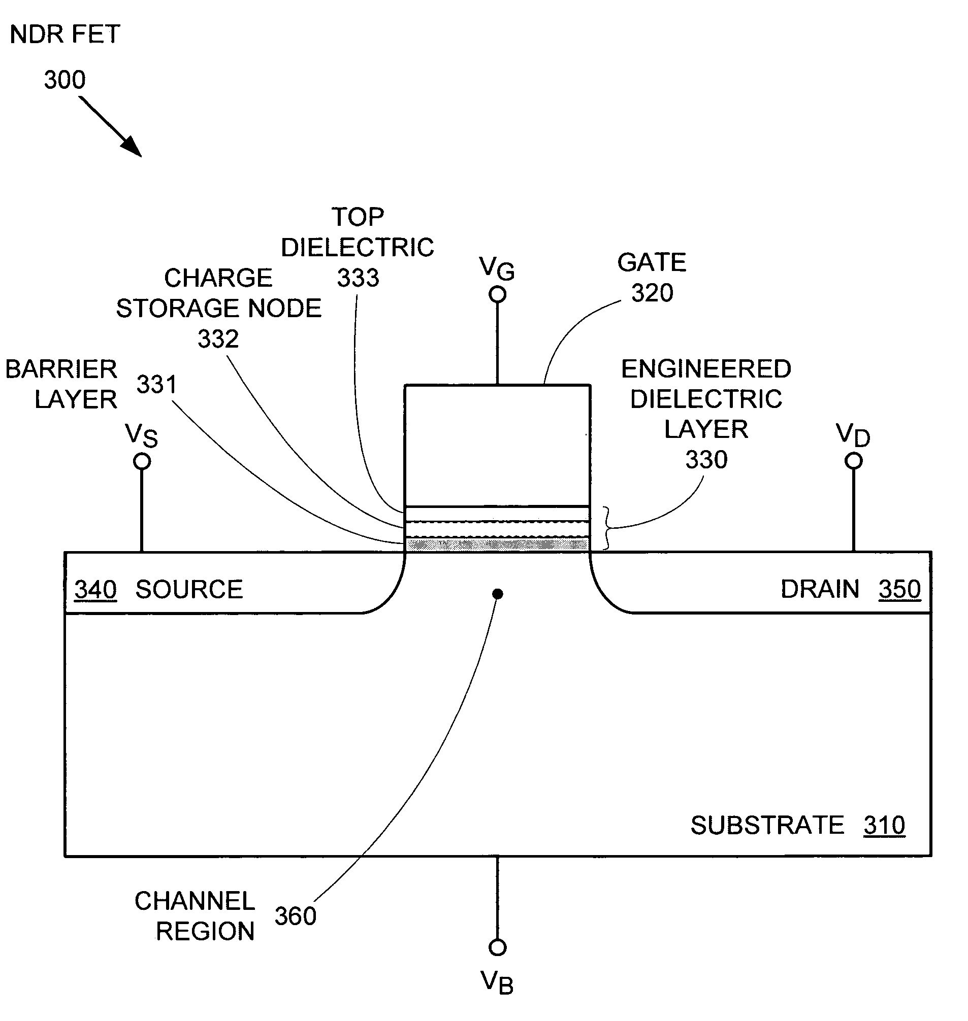
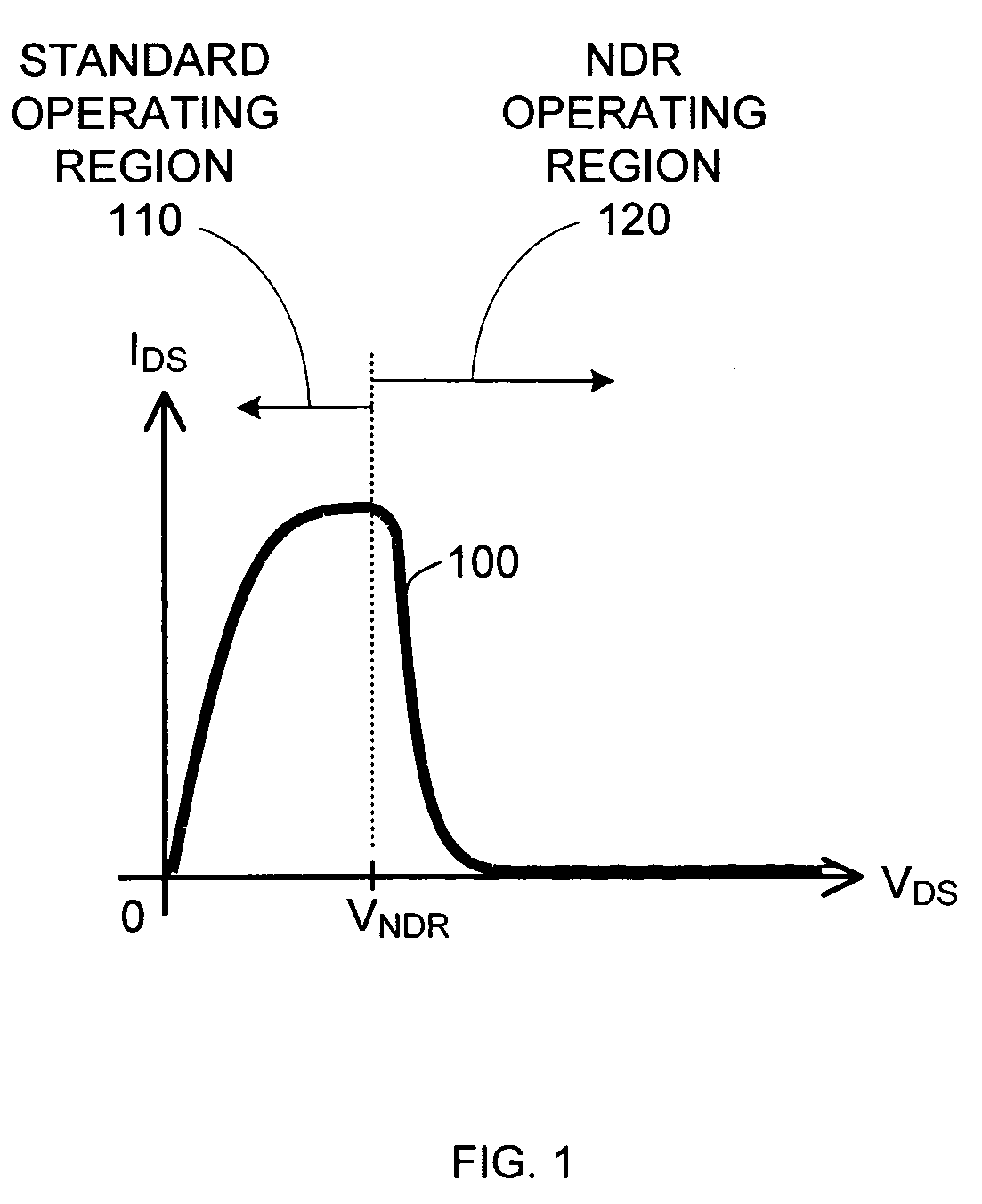
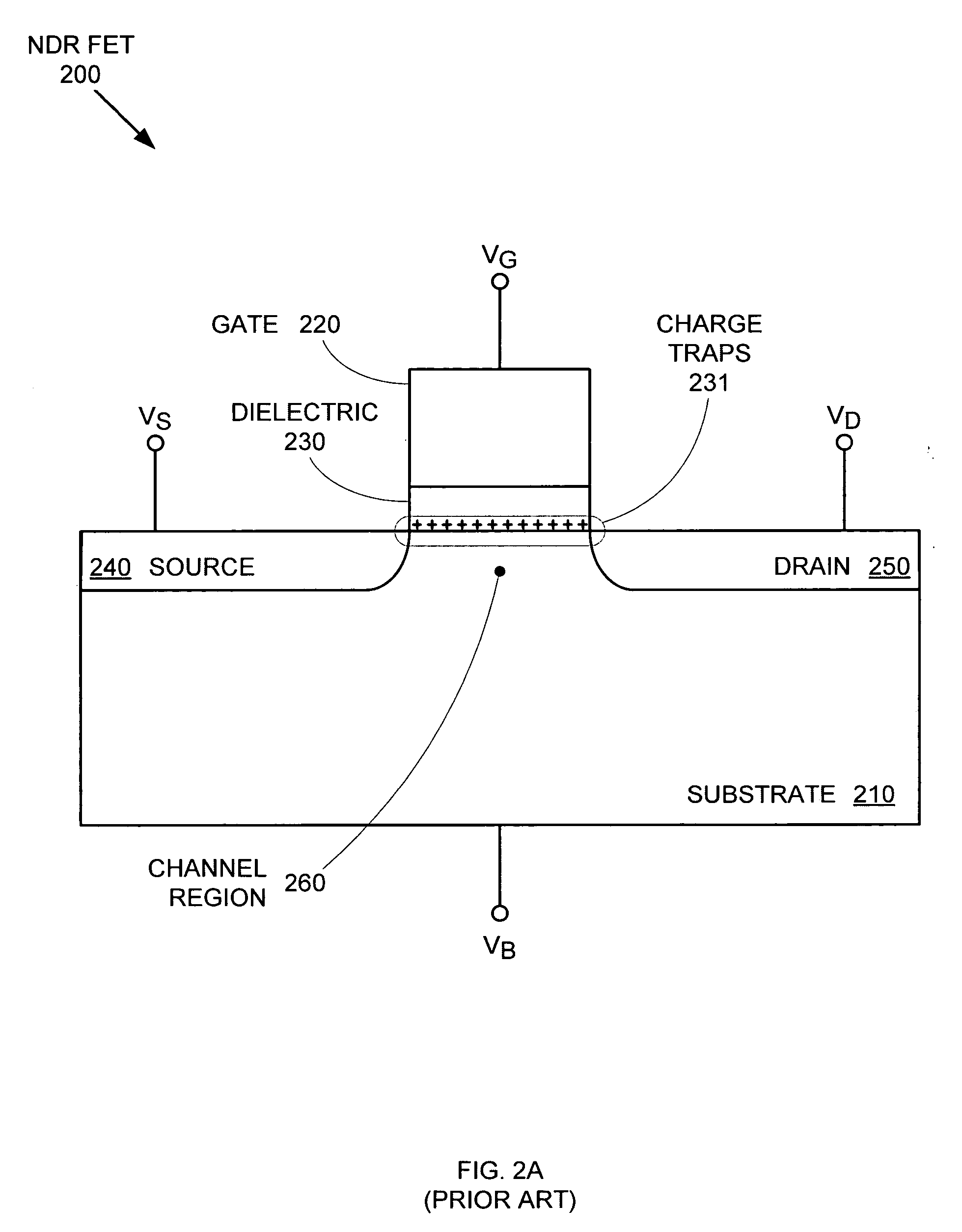
[0023] In a negative differential resistance (NDR) transistor, it is desirable to be able to optimize the device characteristics, such as peak-to-valley ratio (PVR), NDR voltage, for different applications / technologies. In conventional NDR transistors, these characteristics are controlled by the distribution of charge traps at the gate dielectric / channel region interface. However, in certain circumstances, accurately controlling the charge trap distribution, and hence, accurately controlling the PVR, NDR voltage, and / or NDR switching speed values for the NDR transistor, can be difficult. By replacing the charge traps with a barrier layer and a charge storage node (layer) in the gate dielectric, greater manufacturing flexibility and improved control over NDR transistor characteristics can be achieved. As a separate approach, by introducing a gap between the source-channel junction and the gate, the electric field within that gap can be significantly enhanced, thereby improving the PV...


PUM


Abstract

A negative differential resistance (NDR) transistor includes a gate stack formed from a gate, a barrier layer, and a dielectric layer formed between the gate and barrier layer. To enable the NDR characteristic of the transistor, the barrier layer is configured to dynamically transfer charge carriers to and from the channel region of the transistor (e.g., to a charge storage node between the barrier layer and the dielectric layer), thereby adjusting the threshold voltage of the transistor. An NDR transistor can also be formed with a gap between the edge of the source region and the edge of the gate (stack) to enhance the electric field in the portion of the channel region corresponding to the gap. The enhanced electric field can concentrate the distribution of charge carriers removed from the channel region in the proximity of the source region, thereby enhancing the NDR performance of the transistor.

Description

BACKGROUND OF THE INVENTION [0001] 1. Field of the Invention [0002] The invention relates to the field of semiconductor devices, and in particular, to a metal-insulator-semiconductor device that exhibits negative differential resistance behavior. [0003] 2. Related Art [0004] Negative differential resistance (NDR) transistors can beneficially be used in a great number of integrated circuit designs to simplify circuit complexity and improve performance. An NDR transistor is a transistor that exhibits a negative differential resistance characteristic in response to variations in drain-to-source voltage. Specifically, the drain current through the transistor increases with increasing drain-to-source voltage until a threshold voltage (referred to as the “NDR voltage”) is reached, at which point the drain current rapidly decreases with further increases in drain-to-source voltage. [0005]FIG. 1 shows a graph 100 of drain current (i.e., drain-to-source current) IDS for a fixed gate bias vol...

Claims


Application Information

Patent Timeline
Patent Type & Authority Applications(United States)
IPC IPC(8): H01L29/76H01L29/94H01L31/00
CPCH01L21/28273H01L21/28282H01L29/42332H01L29/42348H01L29/517H01L29/7885H01L29/792H01L29/40114H01L29/40117
Inventor LU, QIANGLIU, TSU-JAE KING
Owner SYNOPSYS INC
Why Eureka
Try Eureka