Organic semiconductor device and method of fabricating the same

a technology of organic semiconductors and semiconductor layers, applied in thermoelectric devices, instruments, nanoinformatics, etc., can solve the problems of deteriorating the reliability of memory, affecting the performance of the device, and the manufacturing process is complicated,

Inactive Publication Date: 2007-06-07
ELECTRONICS & TELECOMM RES INST
View PDF26 Cites 17 Cited by
  • Summary
  • Abstract
  • Description
  • Claims
  • Application Information

AI Technical Summary

Benefits of technology

[0019] The step of forming the electron channel layer may comprise the steps of: forming the lower organic layer on the first electrode; forming the nano-particle layer having predetermined sizes of nano-particles that are spaced a predetermined distance apart from each other on the lower organic layer; and forming the upper organic layer on the nano-particle layer. The nano-particle layer, the upper organic layer, and the lower organic layer may be formed by a Langmuir-Blodgett method. The nano-particles may be met

Problems solved by technology

As a result of using such a high voltage, a tunneling oxide layer tends to break down.
This deteriorates the reliability of the memory.
In this case, a fabrication process is very complicated because an equivalent oxide thickness should be considered in design to prevent breakdown of the tunneling oxide layer.
Also, when the flash memory is scaled down to the 65 nm node or less, because of noise between cells, there is a limit to down-scaling a device and the operability of the device comes into question.
In addition, when the current flash memory operates at a low voltage to consume less power, it is

Method used


Image

  • Organic semiconductor device and method of fabricating the same
  • Organic semiconductor device and method of fabricating the same
  • Organic semiconductor device and method of fabricating the same

Examples


Embodiment Construction

[0028] Hereinafter, an organic semiconductor device and a method of fabricating the same according to exemplary embodiments of the present invention will be described in detail with reference to the accompanying drawings.

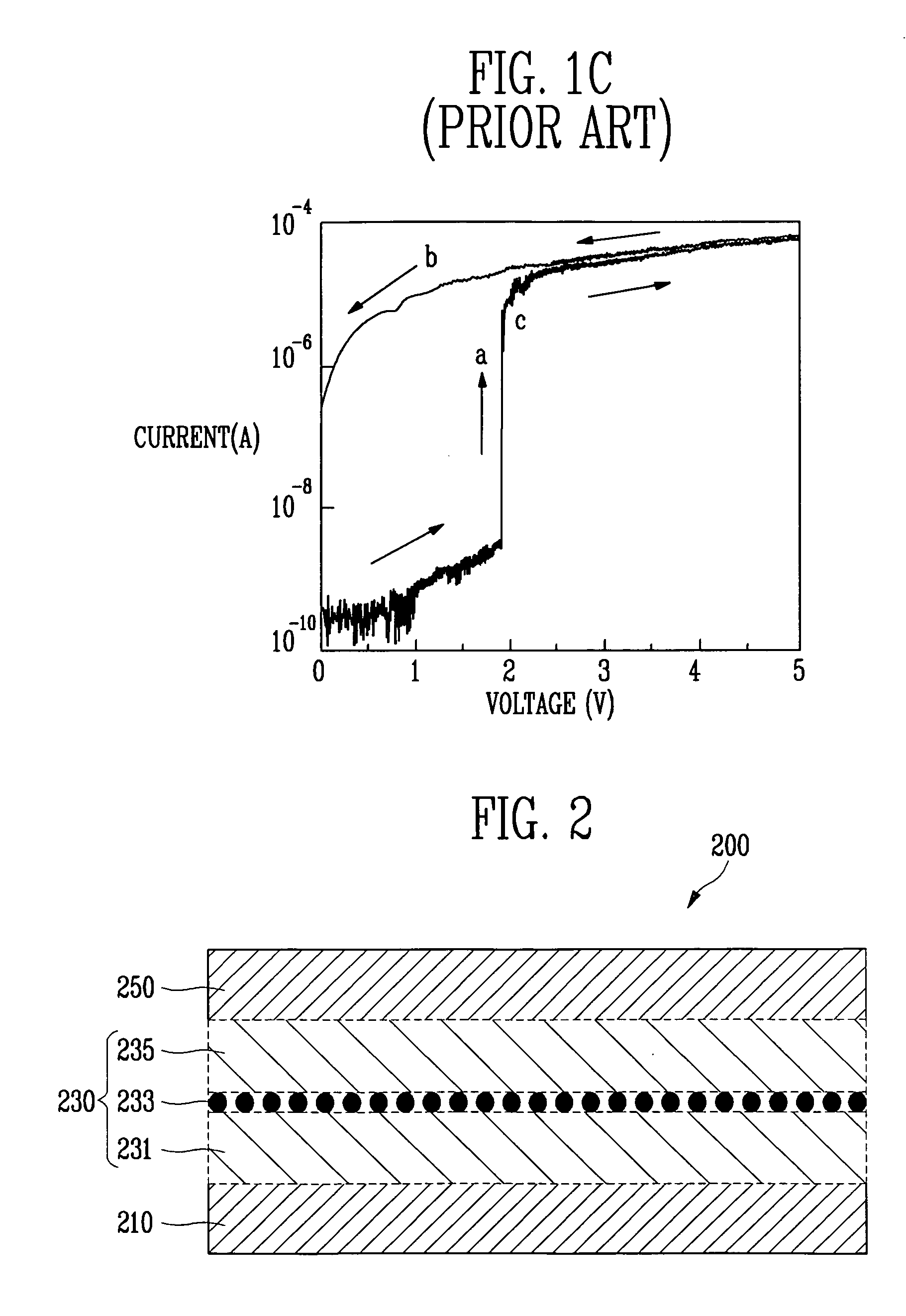
[0029]FIG. 2 illustrates the structure of an organic semiconductor device according to an exemplary embodiment of the present invention. Referring to FIG. 2, an organic semiconductor device 200 according to the present invention includes a first electrode 210, an electron channel layer 230 disposed on the first electrode 210, and a second electrode 250 disposed on the electron channel layer 230. The electron channel layer 230 includes a lower organic layer 231 disposed on the first electrode 210, a nano-particle layer 233 disposed on the lower organic layer 231, and an upper organic layer 235 disposed on the nano-particle layer 233.

[0030] To be specific, the first and second electrodes 210 and 250 may be formed of a general electrode material such as Al, Cu, Au or...


PUM


Abstract

An organic semiconductor device and a method of fabricating the same are provided. The device includes: a first electrode; an electron channel layer formed on the first electrode; and a second electrode formed on the electron channel layer, wherein the electron channel layer comprises: a lower organic layer formed on the first electrode; a nano-particle layer formed on the lower organic layer and including predetermined sizes of nano-particles that are spaced a predetermined distance apart from each other; and an upper organic layer formed over the nano-particle layer. Accordingly, a highly integrated organic semiconductor device can be fabricated by a simple fabrication process, and nonuniformity of devices due to threshold voltage characteristics and downsizing of the device can resolved, so that a semiconductor device having excellent performance can be implemented.

Description

CROSS-REFERENCE TO RELATED APPLICATION [0001] This application claims priority to and the benefit of Korean Patent Applications Nos. 2005-117712 and 2006-35654, filed on Dec. 5, 2005 and Apr. 20, 2006, the disclosure of which is incorporated herein by reference in its entirety. BACKGROUND [0002] 1. Field of the Invention [0003] The present invention relates to an organic semiconductor device and a method of fabricating the same, and more particularly, an organic semiconductor device and a method of fabricating the same including an electron channel layer having a nano-particle layer made of nano-particles. [0004] 2. Discussion of Related Art [0005] Semiconductor device technology has developed to the point of implementation of a Giga-bit DRAM, and it can be expected that a 100 G bit or more integrated circuit will soon be implemented. As semiconductor devices become more integrated, they become smaller in size, more highly functionalized, and have increasingly high-speed, high capac...

Claims


Application Information

Patent Timeline
IPC IPC(8): H01L29/08
CPCB82Y10/00G11C13/00G11C13/0014H01L51/0075H10K85/701
Inventor CHOI, SUNG-YOOLRYU, MIN KIKIM, ANSOONAH, CHIL SEONGYU, HAN YOUNG
Owner ELECTRONICS & TELECOMM RES INST
Why Eureka
Try Eureka