

Heat insulating stamper structure
- Summary
- Abstract
- Description
- Claims
- Application Information
AI Technical Summary
Benefits of technology
Problems solved by technology
Method used
Image

Examples
embodiment
First Embodiment
Structure and Example of Layer Specification
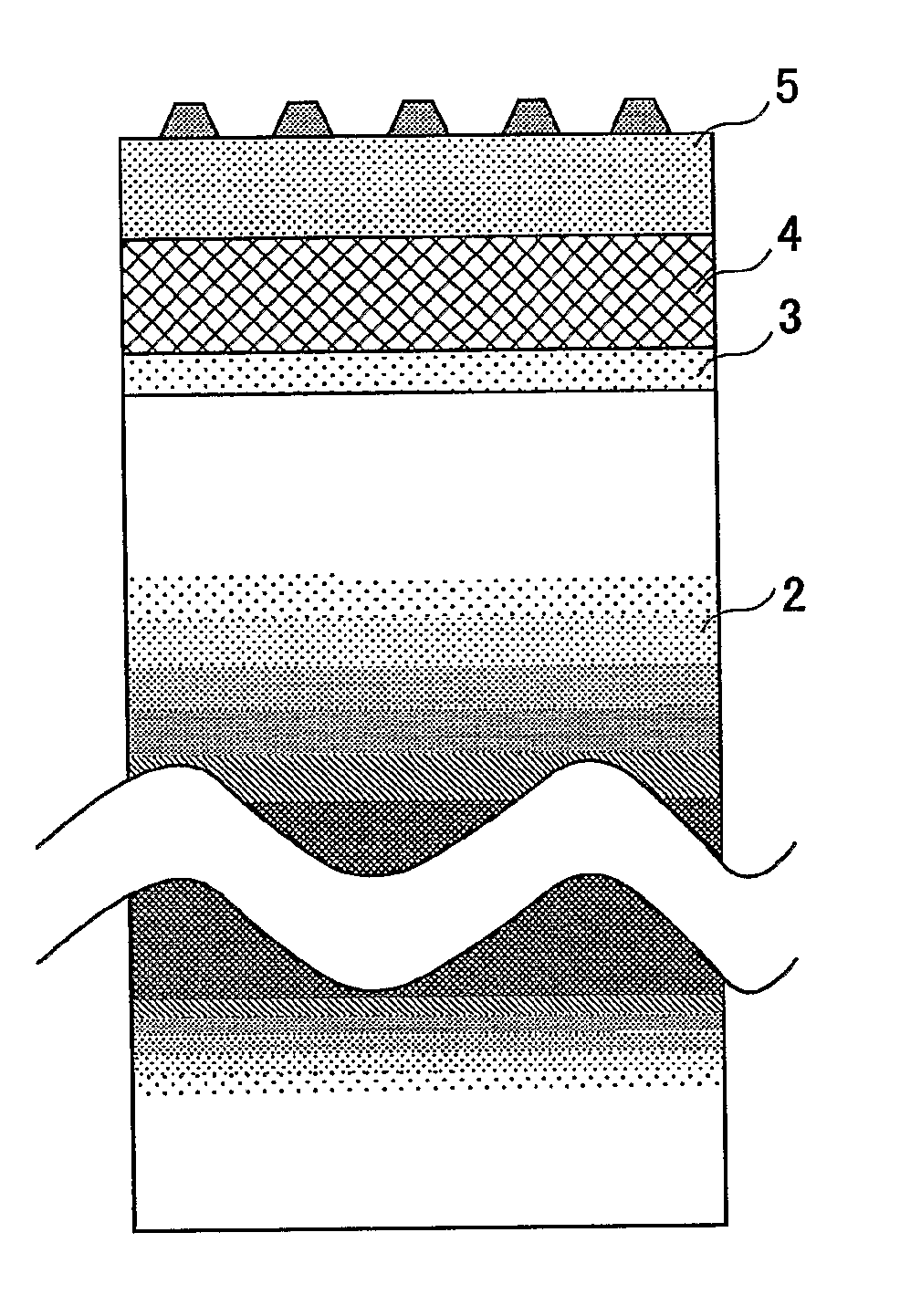
[0067]FIG. 7: Since the stamper of the present invention comprises mainly metallic Ni, the strength problem is solved.
[0068] Accordingly, the primary plating layer 5 may be made very thin so as to reduce the heat capacity and increase temperature rising speed.
[0069] The thickness of the composite Ni plating layer 9 of FIG. 7 may be determined based on the heat conductivity.
[0070] Ni has a heat conductivity 10 or more times higher than the resins (Teflon™, polyamide) . That is, when the plating layer 5 of the present invention has a thickness of 1 / 10 times of that of the related-art plating layer 5, the composite material heat insulating layer of the present invention offers the same performance as the related-art heat insulating layer. Moreover, the reduction of the thickness of the primary plating layer 5 can reduce the production time.
[0071] The primary plating layer 5 of the present invention shown in FIG. 7 may be...
second embodiment
Example of Insulating Layer Formation (PTFE and Polyimide Dispersion Electroplating)
[0094] The following is an electroplating bath composition used in this embodiment. [0095] sulfamic acid Ni solution (1 mol / L), Ni chloride solution (0.2 mol / L), fluoboric acid (0.5 mol / L) [0096] sulfamic acid Ni (280 g / L), Ni chloride (45 g / L), fluoboric acid (40 g / L): Watt bath
[0097] PTFE or polyimide particles of a particle diameter of 10-500 nm (10-40 g / L) are added together with dispersion aid and stirred, and pre-plating is performed for initial make-up of electrolytic bath.
[0098] The temperature of the bathing fluid may be set to within a range of 55° C. through room temperature, preferably to 40° C. If the temperature is too high, cracking may occur in a plating film.
[0099] A master stamper subjected to a separation film treatment is opposed by a Ni anode such that a Ni conductive film is formed on the master stamper by sputtering of 800 Å or electroless plating. Then an anode with Ni pel...
third embodiment 3
Example of Simplification of Entire Process
[0102]FIG. 8 shows a process flow disclosed in Patnt Document 5.
[0103] In the process flow, a step “5. son stamper production: primary plating / polymer layer formation / conduction processing / secondary plating formation” is related to a related-art heat insulating son stamper.
[0104] Manufacturing machines used in this step are an electroforming apparatus (cleaning / drying), a resin blender, a spinner (resin application), a high-15 temperature reactor (resin curing), an etch apparatus (surface roughening), a sputtering apparatus (conductive film formation), and an electroforming apparatus.
[0105] On the other hand, the present invention only uses a first electroforming apparatus 1 (Ni plating bath) and a second electroforming apparatus 2 (composite dispersion plating bath). Consequently, the energy consumption is reduced by about 50%.
[0106] The same may apply to steps “3. master stamper production” and “4. mother stamper production” shown i...
PUM
| Property | Measurement | Unit |
|---|---|---|
| Electrical conductivity | aaaaa | aaaaa |
| Concentration | aaaaa | aaaaa |
| Heat | aaaaa | aaaaa |
Abstract
Description
Claims
Application Information