Emissive device, process for producing emissive device, and electronic apparatus

a technology of emissive devices and electronic devices, which is applied in the direction of discharge tubes/lamp details, discharge tubes luminescnet screens, electric discharge lamps, etc., can solve the problems of reducing the lifetime reducing the efficiency of the luminescent device, and difficult to prevent the permeation of water and oxygen with the bonded seal alone, so as to improve production efficiency and reduce production costs

Active Publication Date: 2007-06-14
SEIKO EPSON CORP
View PDF7 Cites 73 Cited by
  • Summary
  • Abstract
  • Description
  • Claims
  • Application Information

AI Technical Summary

Benefits of technology

[0027] The first inorganic layer is composed of a material having an elastic modulus of 10 to 100 GPa. Thus, the occurrence of a crack in or detachment of the second electrode and the second inorganic layer can be surely prevented.
[0028] The first inorganic layer and the second inorganic layer are succes

Problems solved by technology

Many materials used for luminescent layers, hole-injection layers, and electron-injection layers of organic EL devices easily react with moisture in the atmosphere and degraded.
Degradation of these layers causes the formation of a nonluminous region, which is referred to as “dark spot”, in an organic EL device, thus reducing the lifetime of the luminescent device.
Accordingly, an important issue in designing of such organic EL devices is to suppress effects of moisture, oxygen, and the like.
However, trends toward larger screens and reductions in thickness and weight of organic EL devices make it difficult to prevent the permeation of water and oxygen with

Method used


Image

  • Emissive device, process for producing emissive device, and electronic apparatus
  • Emissive device, process for producing emissive device, and electronic apparatus
  • Emissive device, process for producing emissive device, and electronic apparatus

Examples


first embodiment

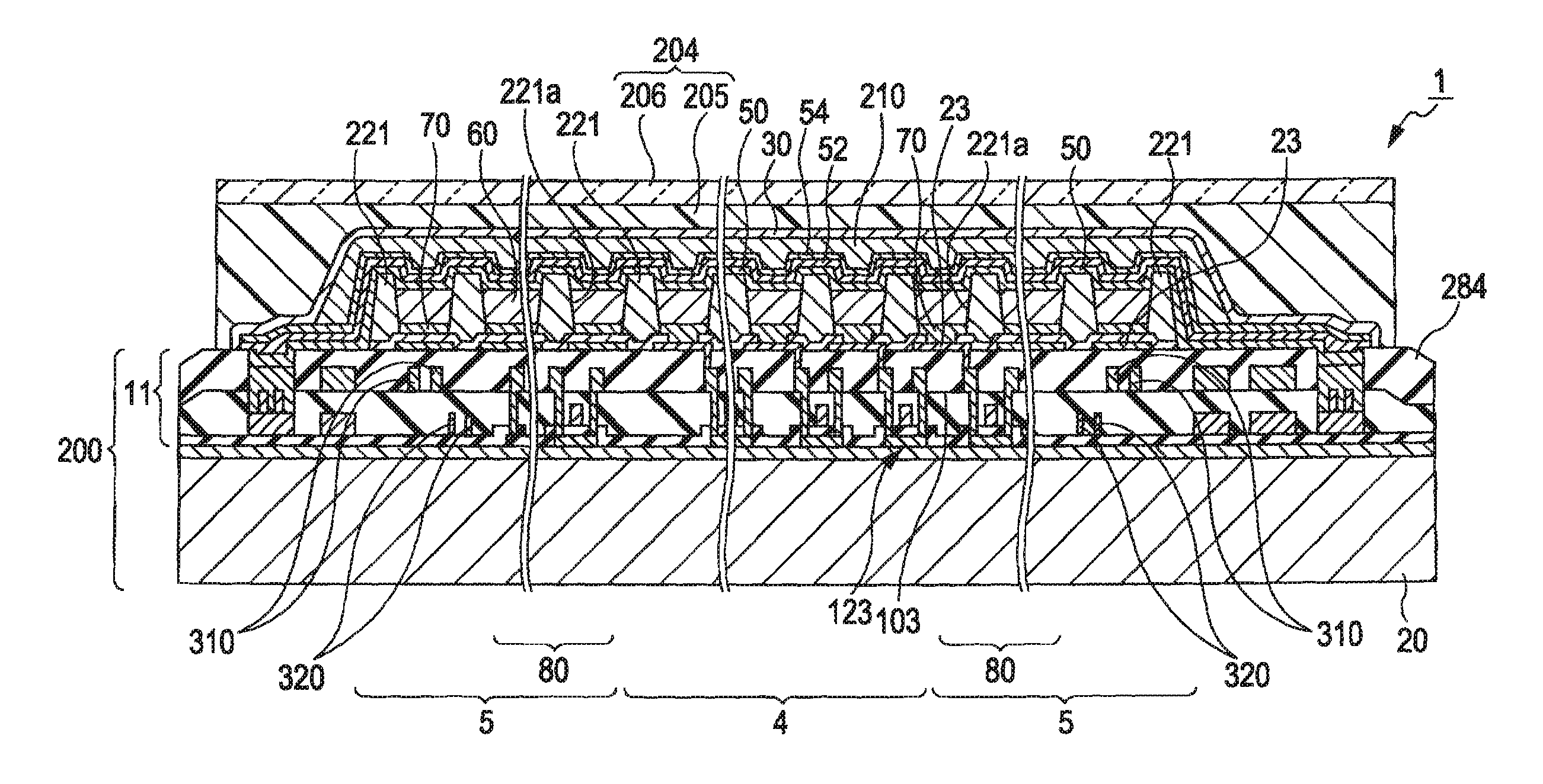
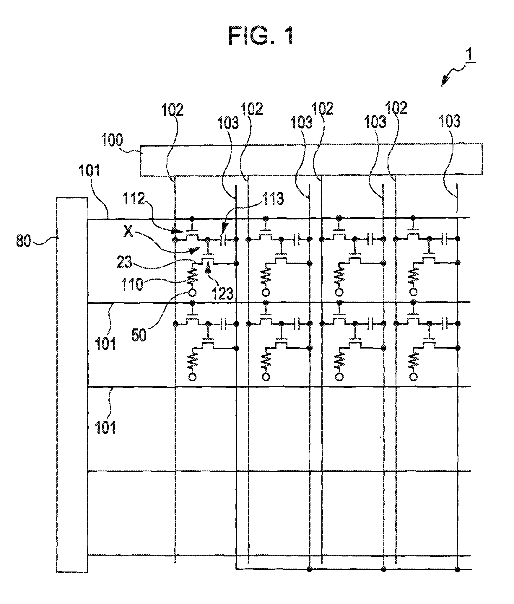
[0045]FIG. 1 shows the wiring structure of an EL display 1 according to a first embodiment of the invention.

[0046] The EL display 1 (emissive device) is of an active matrix type including thin-film transistors (hereinafter, referred to as “TFTs”) as switching elements.

[0047] Hereinafter, portions and layers constituting the EL display 1 are shown at different scales so as to be recognizable in the drawings.

[0048] The EL display 1 includes a plurality of scan lines 101; a plurality of signal lines 102 extending perpendicularly to the scan lines 101; a plurality of power lines 103 extending in parallel with the signal lines 102; and pixel regions X disposed in the vicinity of intersections of each scan line 101 and the corresponding signal line 102.

[0049] The signal lines 102 are connected to a data-line-driving circuit 100 including a shift resister, a level shifter, a video line, and an analog switch. The scan lines 101 are connected to a scan-line-driving circuit 80 having a sh...

second embodiment

[0158] An EL display 2 according to a second embodiment of the invention will be described below. In this embodiment, the same elements as the first embodiment are designated using the same reference numerals, and redundant description is not repeated.

[0159]FIG. 9 is a schematic cross-sectional view of the EL display 2 according to the second embodiment of the invention. FIG. 10 is an enlarged view showing an end (peripheral region) of the organic buffer layer 210 in the EL display 2.

[0160] The EL display 2 differs from the EL display 1 according to the first embodiment in that a white-light-emitting layer 60W that emits white light is used as the luminescent layer; and a color filter substrate 207 is used as the surface-protecting substrate.

[0161] Examples of a white-light-emitting organic material include a styrylamine-based luminescent material and an anthracene-based dopamine (blue); and a styrylamine-based luminescent material and a rubrene-based dopamine (yellow).

[0162] A ...

example

[0176] The presence or absence of the occurrence of a defect when the first cathode-protecting layer 52 and the second cathode-protecting layer 54 are disposed on the cathode 50 will be described below.

[0177]FIG. 11 is a table showing the presence or absence of the occurrence of a defect when the first cathode-protecting layer 52 is disposed on the organic banks 221 having a bump of about 3 μm, the luminescent layer 60 covering the organic banks 221 and having a mutilayer structure, and the cathode 50 composed of a magnesium-silver alloy and having a thickness of 10 nm.

[0178] Specifically, the first cathode-protecting layer 52 was formed with any one of the materials described in FIG. 11. When the second cathode-protecting layer 54, the organic buffer layer 210, and the gas barrier layer 30 were laminated, the presence or absence of the occurrence of a defect in the cathode 50 or the second cathode-protecting layer 54 was checked. In particular, whether or not detachment or a crac...


PUM


Abstract

An emissive device includes a substrate; a plurality of first electrodes; pixel banks having a plurality of openings each corresponding to the position of a corresponding one of the first electrodes; organic function layers disposed in at least the openings; a second electrode disposed so as to cover the pixel banks and the organic function layers; a first inorganic layer disposed over the second electrode; a second inorganic layer disposed over the first inorganic layer; an organic buffer layer disposed over the second inorganic layer; and a gas barrier layer disposed over the organic buffer layer.

Description

BACKGROUND [0001] 1. Technical Field [0002] The present invention relates to an emissive device, a process for producing the emissive device, and an electronic apparatus. [0003] 2. Related Art [0004] In recent years, demands for flat displays having lower power consumption and less weight have been increasing with diversification and the like of information equipment. Organic electroluminescfent (EL) devices having luminescent layers are one known example of the flat displays. Typically, the organic EL devices each have a structure in which the luminescent layer is disposed between an anode and a cathode. To improve hole-injection properties and electron-injection properties, a structure in which a hole-injection layer is disposed between the anode and the luminescent layer and a structure in which an electron-injection layer is disposed between the luminescent layer and the cathode have been developed. [0005] Many materials used for luminescent layers, hole-injection layers, and el...

Claims


Application Information

Patent Timeline
IPC IPC(8): H05B33/04H01J1/62
CPCH01L27/3244H01L51/5237H10K59/12H10K50/841H10K50/844H05B33/04
Inventor HAYASHI, KENJIYAMAUCHI, YUKIO
Owner SEIKO EPSON CORP
Why Eureka
Try Eureka