Optical device coupling light propagating in optical waveguide with diffraction grating

a technology of optical waveguide and coupling grating, which is applied in the direction of optical waveguide light guide, optical resonator shape and construction, and semiconductor lasers. it can solve the problems of reducing optical output and increasing power consumption, and achieve the effect of raising the coupling coefficient between light and dark

Active Publication Date: 2007-06-14
FUJITSU LTD
View PDF14 Cites 59 Cited by
  • Summary
  • Abstract
  • Description
  • Claims
  • Application Information

AI Technical Summary

Benefits of technology

[0031] As the refractive index of the upper clad layer is set higher than that of the lower clad layer, the intensity of light in a region above the active layer becomes strong. It is therefore possible to raise the coupling coefficient between light and diffraction gratings.

Problems solved by technology

Making the ridge 503 thinner results in an increase in power consumption and a reduction of optical output to be caused by heat generation during large current injection.

Method used


Image

  • Optical device coupling light propagating in optical waveguide with diffraction grating
  • Optical device coupling light propagating in optical waveguide with diffraction grating
  • Optical device coupling light propagating in optical waveguide with diffraction grating

Examples


first embodiment

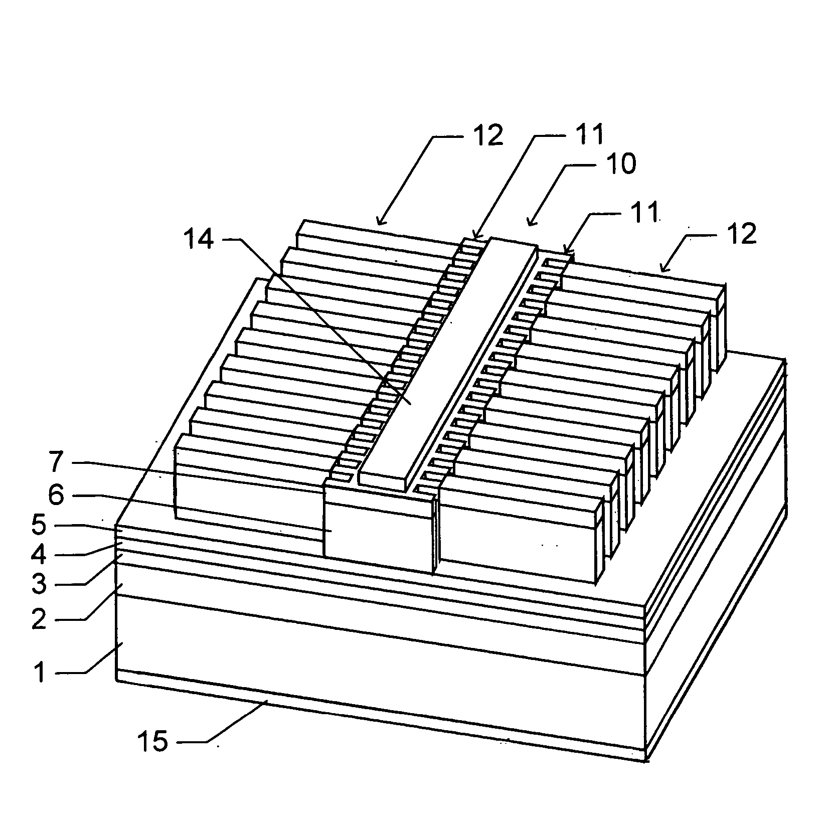
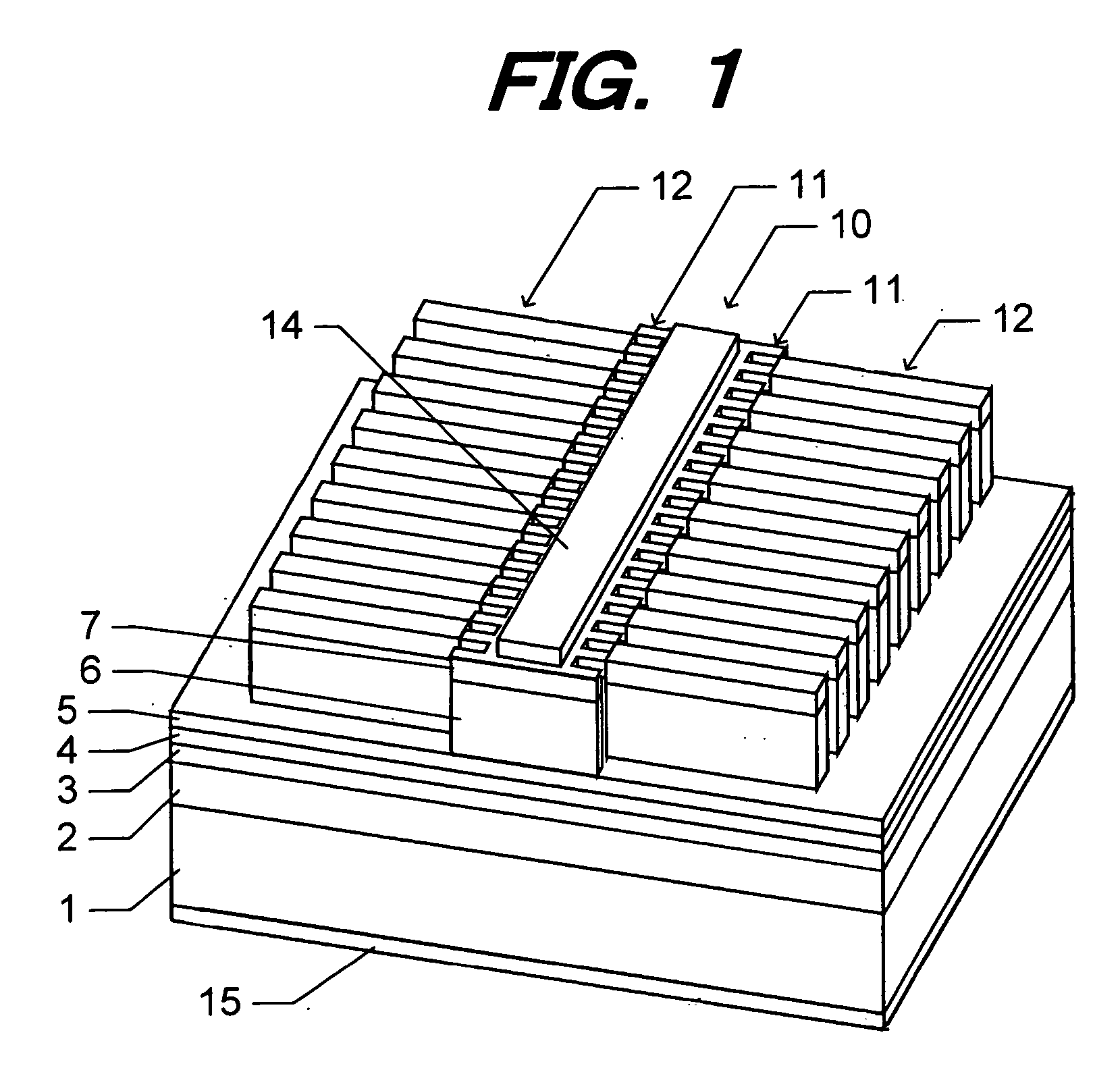
[0061]FIG. 1 is a perspective view of a ridge-waveguide DFB laser diode according to the A lower clad layer 2 of n-type Al0.5Ga0.5As having a thickness of 1.5 μm, a lower optical guide layer 3 of n-type Al0.3Ga0.7As having a thickness of 0.15 μm, a quantum dot active layer (optical waveguide layer) 4 and an upper optical guide layer 5 of p-type Al0.3Ga0.7As having a thickness of 0.15 μm are stacked in this order on the principal surface of a substrate 1 of n-type GaAs are.

[0062] The quantum dot active layer 4 has a lamination structure having ten repeating units, each of which has an InGaAs layer containing a number of quantum dots of InAs and GaAs layers sandwiching the InGaAs layer, the ten repeating units being stacked in the thickness direction.

[0063] A ridge 10 having a height of 1.4 μm and a width of 2 μm elongated in one direction is disposed on the upper optical guide layer 5. A main diffraction grating 11 is formed on both side surfaces of the ridge 10, the main diffracti...

second embodiment

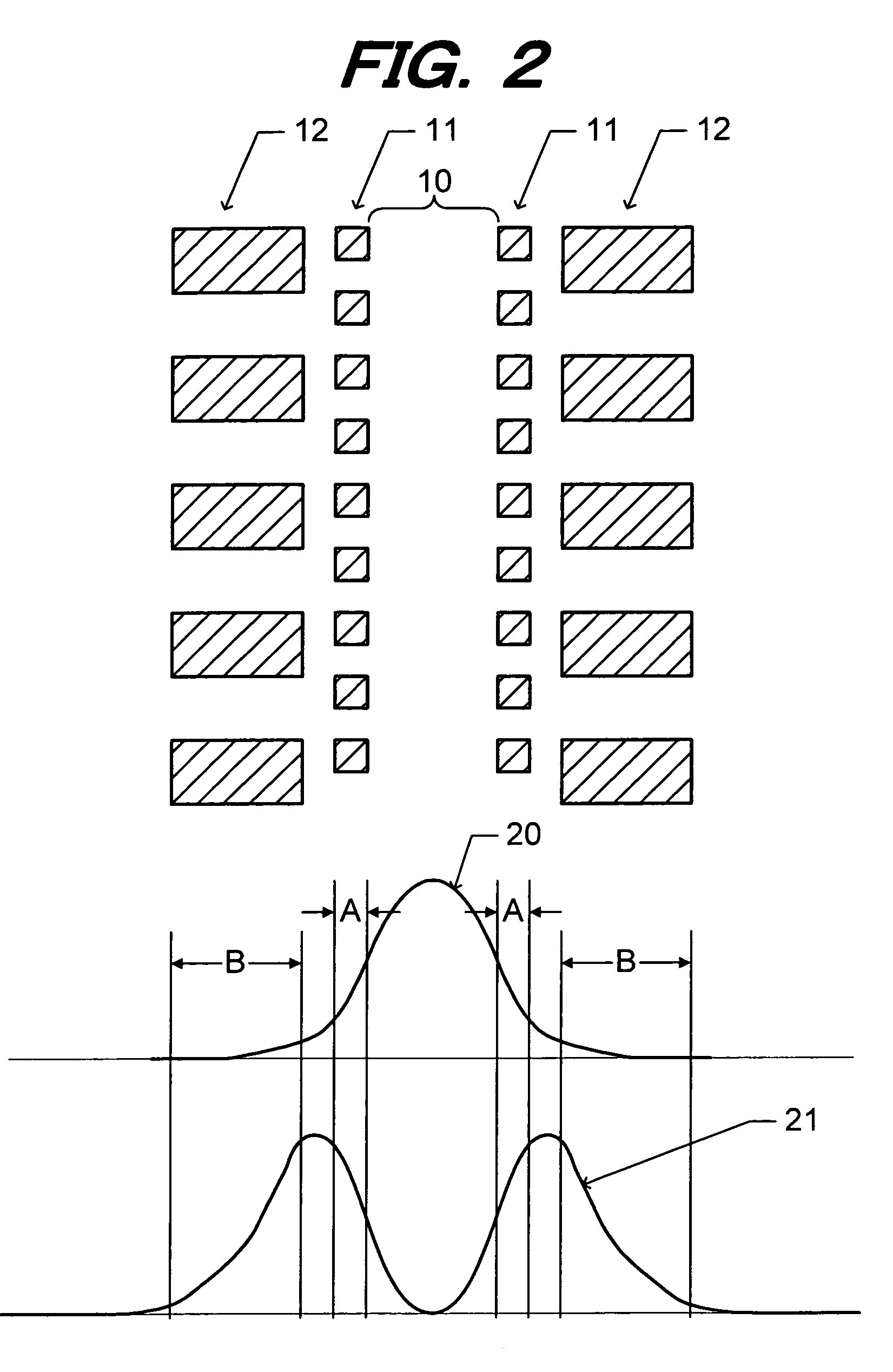
[0107] The second embodiment utilizes a mutual phase shift of two diffraction light diffracted by the two portions of the sub-diffraction grating 12A and propagating in the optical waveguide in a propagation direction. It is therefore preferable to design the sub-diffraction grating 12A in such a manner that a diffraction intensity of light in the propagation direction becomes high. As indicated by the curve d shown in FIG. 3, the diffraction intensity of light in the propagation direction reaches its maximum value at the duty ratios of 25% and 75%. In order to increase the diffraction intensity of light in the propagation direction, it is preferable to set the duty ratio of the sub-diffraction grating in a range of 15 to 35% or in a range of 65 to 85%.

[0108] Also in the second embodiment, as in the case of the modification of the first embodiment shown in FIG. 5, the lower guide layer 3 may be omitted to directly contact the lower clad layer 2 to the active layer 4. The conductivit...

fourth embodiment

[0116]FIG. 11 is a perspective view of a ridge-waveguide DFB laser diode according to the A main diffraction grating 60 constituted of periodically disposed convex and concave portions is formed on the principal surface of a substrate 51 of n-type InP. An optical guide layer 52 of n-type GaInAsP having a thickness of 0.1 μm is formed on the surface of the main diffraction grating 60.

[0117] A quantum well active layer 53 is formed on the optical guide layer 52. The quantum well active layer 53 has the structure that a quantum well layer of undoped AlGaInAs having a thickness of 6 nm and a barrier layer of undoped AlGaInAs having a thickness of 10 nm are alternately laminated ten times and this alternate lamination structure is sandwiched between guide layers of undoped AlGaInAs having a thickness of 20 nm. A composition wavelength of AlGaInAs constituting the barrier layers and guide layers is 1050 nm.

[0118] An upper clad layer 54 of p-type InP is formed on the quantum well active ...


PUM


Abstract

An optical waveguide propagates a laser beam. Main diffraction grating and sub-diffraction grating couple light propagating in the optical waveguide. The main diffraction grating and the sub-diffraction grating couple the light in such a manner that propagation in a second order transverse mode of the light propagating in the optical waveguide when both the main diffraction grating and the sub-diffraction grating are disposed, is suppressed more than propagation in the second order transverse mode of the light propagating in the optical waveguide when only the main diffraction grating is disposed.

Description

CROSS REFERENCE TO RELATED APPLICATION [0001] This application is based on and claims priority of Japanese Patent Applications No. 2006-038840 filed on Feb. 16, 2006 and No. 2005-355992 filed on Dec. 9, 2005, the entire contents of which are incorporated herein by reference. BACKGROUND OF THE INVENTION [0002] A) Field of the Invention [0003] The present invention relates to an optical device in which light propagating in an optical waveguide is made to have a narrow spectrum by coupling the light with diffraction gratings. [0004] The present invention further relates to an optical device having the structure of raising a coupling coefficient between light propagating in an optical waveguide and diffraction gratings. [0005] B) Description of the Related Art [0006] With a tremendous increase in Internet demands, efforts geared to ultra high speed and large capacity optical communication and optical transmission are intensified. For the Ethernet (registered trademark) having more than ...

Claims


Application Information

Patent Timeline
Patent Type & Authority Applications(United States)
IPC IPC(8): H01S3/08H01S5/12
CPCB82Y20/00H01S5/0655H01S5/12H01S5/1231H01S5/1237H01S5/125H01S5/22H01S5/227H01S5/3412G02B6/10G02B5/18
Inventor MATSUDA, MANABUYAMAMOTO, TSUYOSHI
Owner FUJITSU LTD
Why Eureka
Try Eureka