Method of manufacturing non-volatile memory element

a non-volatile memory element, electrically rewritable technology, applied in the direction of basic electric elements, electrical apparatus, semiconductor devices, etc., can solve the problems of heat generation efficiency decline and problems such as rewriting current, and achieve the effect of reducing rewriting current, increasing heat generation efficiency, and reducing rewriting curren

Inactive Publication Date: 2007-06-21
ELPIDA MEMORY INC
View PDF7 Cites 15 Cited by
  • Summary
  • Abstract
  • Description
  • Claims
  • Application Information

AI Technical Summary

Benefits of technology

[0017] In the present invention, the phase change material preferably contains a chalcogenide material. Ge2Sb2Te5 (GST) is especially preferred as the chalcogenide material. When nitrogen is added to Ge2Sb2Te5, the crystal grain size becomes smaller than in conventional Ge2Sb2Te5. The crystal grain boundary also increases, allowing diffusion of the adhesion layer into the Ge2Sb2Te5 to be more readily performed. It is believed that performing a heat treatment and supplying a rewriting current causes the adhesion layer to diffuse gradually into the recording layer along the boundary of the grains that constitute the recording layer, and the effect of the adhesion layer to ultimately disappear. Additionally, since the resistivity of Ge2Sb2Te5 with added nitrogen is larger than the resistivity of Ge2Sb2Te5 without any additive, an effect is also observed wherein the rewriting current is reduced.
[0018] In the present invention, the fourth step preferably includes a step for performing a heat treatment at a prescribed temperature. The prescribed temperature is preferably 350° C. or more. It is believed that when a heat treatment is performed, the elements constituting the adhesion layer gradually diffuse into the recording layer along the grain boundary of t...

Problems solved by technology

Therefore, problems have arisen insofar...

Method used


Image

  • Method of manufacturing non-volatile memory element
  • Method of manufacturing non-volatile memory element
  • Method of manufacturing non-volatile memory element

Examples


first embodiment

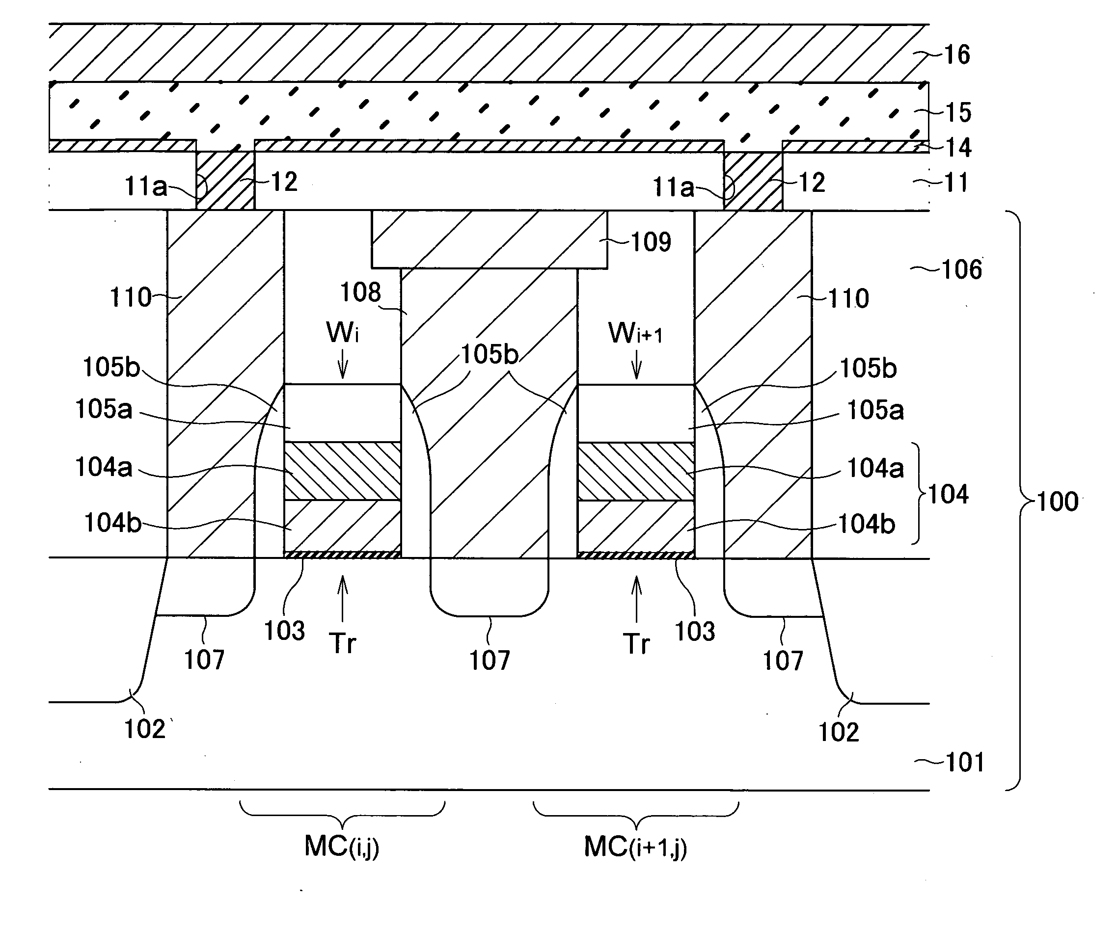
[0063] In the first embodiment described above, the adhesion layer 14 is diffused into the recording layer 15. Therefore, nitrogen is added to the GST or other chalcogenide material that constitutes the recording layer 15, and diffusion of the Ti that constitutes the adhesion layer 14 is induced by subsequent heat treatments. However, an adequate resistance ratio between the crystalline phase and the amorphous phase can be obtained using a chalcogenide material with no added nitrogen. Such a method will be explained in detail below.

[0064]FIG. 13 is a flowchart showing a method of manufacturing a non-volatile memory element according to a second preferred embodiment of the present invention.

[0065] As shown in FIG. 13, in the manufacture of a non-volatile memory element according to the present embodiment, first, a non-volatile memory element having a recording layer 15 without added nitrogen is formed (S101). The non-volatile memory element can be manufactured according to the manuf...

second embodiment

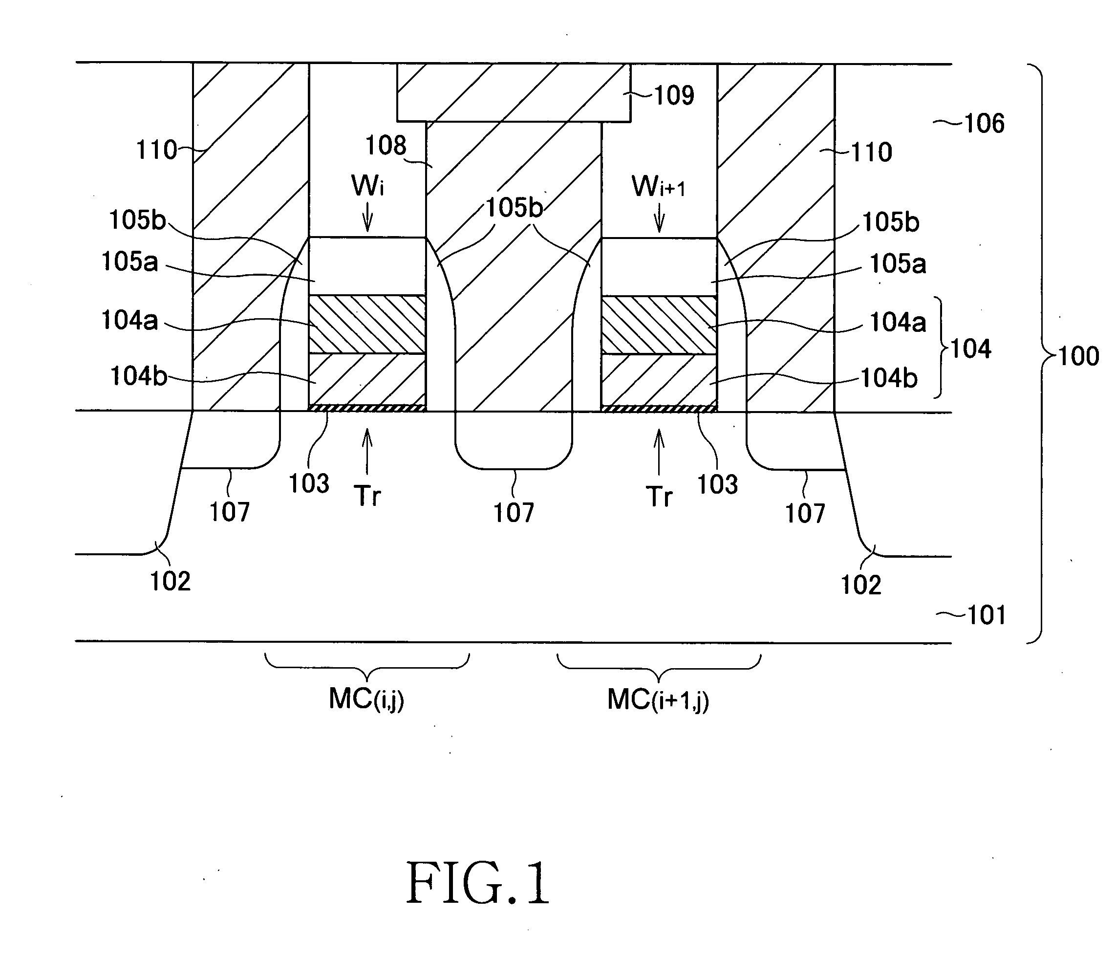
[0074] In the second embodiment described above, the adhesion layer 14 only above the lower electrode 12 is vanished by performing the initializing process of non-volatile memory element having the recording layer without added nitrogen. However, the adhesion layer 14 above the lower electrode 12 may be removed by photolithography and dry-etching after laminating the adhesion layer 14.

[0075]FIG. 16 is a flowchart showing a method of manufacturing a non-volatile memory element according to a third preferred embodiment of the present invention.

[0076] As shown in FIG. 16, in the manufacture of a non-volatile memory element according to the present embodiment, first, an adhesion layer 14 without added nitrogen is formed (S201). The adhesion layer 14 is formed on an interlayer insulating film 11 so that an electrical connection is established with a lower electrode 12. Next, the adhesion layer 15 above the lower electrodes 12 is partially removed by photolithography and dry-etching (S20...


PUM


Abstract

A method of manufacturing a non-volatile memory element in the present invention comprises a first step for forming an adhesion layer on an interlayer insulating film so that an electrical connection is established with a lower electrode, a second step for forming a recording layer containing a phase change material on the adhesion layer, a third step for forming an upper electrode that is electrically connected to the recording layer, and a fourth step for diffusing in the recording layer some of the adhesion layer positioned between at least the lower electrode and the recording layer.

Description

TECHNICAL FIELD [0001] The present invention relates to a method of manufacturing an electrically rewritable non-volatile memory element, and particularly relates to a method of manufacturing a non-volatile memory element having a recording layer that includes phase change material. BACKGROUND OF THE INVENTION [0002] Personal computers and servers and the like use a hierarchy of memory devices. There is lower-tier memory, which is inexpensive and provides high storage capacity, while memory higher up the hierarchy provides high-speed operation. The bottom tier generally consists of magnetic storage such as hard disks and magnetic tape. In addition to being non-volatile, magnetic storage is an inexpensive way of storing much larger quantities of information than solid-state devices such as semiconductor memory. However, semiconductor memory is much faster and can access stored data randomly, in contrast to the sequential access operation of magnetic storage devices. For these reasons...

Claims


Application Information

Patent Timeline
IPC IPC(8): H01L21/336
CPCH01L27/2436H01L27/2472H01L45/06H01L45/1233H01L45/126H01L45/143H01L45/144H01L45/148H01L45/1625H01L45/1658H10B63/30H10B63/82H10N70/231H10N70/826H10N70/8413H10N70/8825H10N70/8828H10N70/884H10N70/026H10N70/046
Inventor KAWAGOE, TSUYOSHIASANO, ISAMU
Owner ELPIDA MEMORY INC
Why Eureka
Try Eureka