Semiconductor light emitting device and method of manufacturing the same

a technology of semiconductor and light-emitting devices, which is applied in the direction of semiconductor/solid-state device manufacturing, semiconductor devices, electrical equipment, etc., can solve the problems of low electrical contact properties, low reflectivity, and low reflectivity, so as to improve the linearity of light reflection and semiconductor layers, high reflectivity, and high reflectivity

Inactive Publication Date: 2007-06-28
SONY CORP
View PDF1 Cites 38 Cited by
  • Summary
  • Abstract
  • Description
  • Claims
  • Application Information

AI Technical Summary

Benefits of technology

[0012] In the semiconductor light emitting device and the method of manufacturing a semiconductor light emitting device according to the embodiment of the invention, when the light reflection layer is deposited on the surface of the second conductive layer, the transparent substrate, and by extension to the semiconductor layer is heated at the first temperature range. Thereby, the disturbance of the crystal regularity in an interface with the light reflection layer in the second conductive layer is prevented, and in a state where moisture and an organic component is prevented from being deposited on the interface, the light reflection layer can be deposited on the surface of the second conductive layer. After that, the semiconductor layer and the light reflection layer are heated in a predetermined time range at an ambient temperature within the second temperature range higher than the first temperature range. Thereby, Ag included in the light reflection layer is dispersed into the second conductive layer to form a compound. As a result, the light reflection layer makes ohmic contact with the semiconductor layer, so the linearity of the light reflection layer and the semiconductor layer is increased. In addition, the light reflection layer includes Ag with extremely high reflectivity.
[0013] In the semiconductor light emitting device and the method of manufacturing a semiconductor light emitting device according to the embodiment of the invention, after the light reflection layer including Ag and the predetermined material is deposited on the surface of the second conductive layer while heating the transparent substrate at the first temperature range, the semiconductor layer and the light reflection layer are heated in a predetermined time range at an ambient temperature within the second temperature range higher than the first temperature range, so the light reflection layer makes ohmic contact with the semiconductor layer, and the light reflection layer can reflect light emitted from the semiconductor layer with high reflectivity. Thereby, a semiconductor light emitting device having high reflectivity and a high electrical contact property between the light reflection layer and the semiconductor layer can be achieved.

Problems solved by technology

However, as a layer made of a material with low reflectivity is arranged between a light reflection layer and a semiconductor layer, the reflectivity declines inevitably, thereby high reflectivity is not expected.
However, even if the light reflection layer is simply heated at a low temperature, a schottky contact is hardly changed into an ohmic contact, so the electrical contact property is still low.

Method used


Image

  • Semiconductor light emitting device and method of manufacturing the same
  • Semiconductor light emitting device and method of manufacturing the same
  • Semiconductor light emitting device and method of manufacturing the same

Examples


Embodiment Construction

[0022] A preferred embodiment will be described in detail below referring to the accompanying drawings.

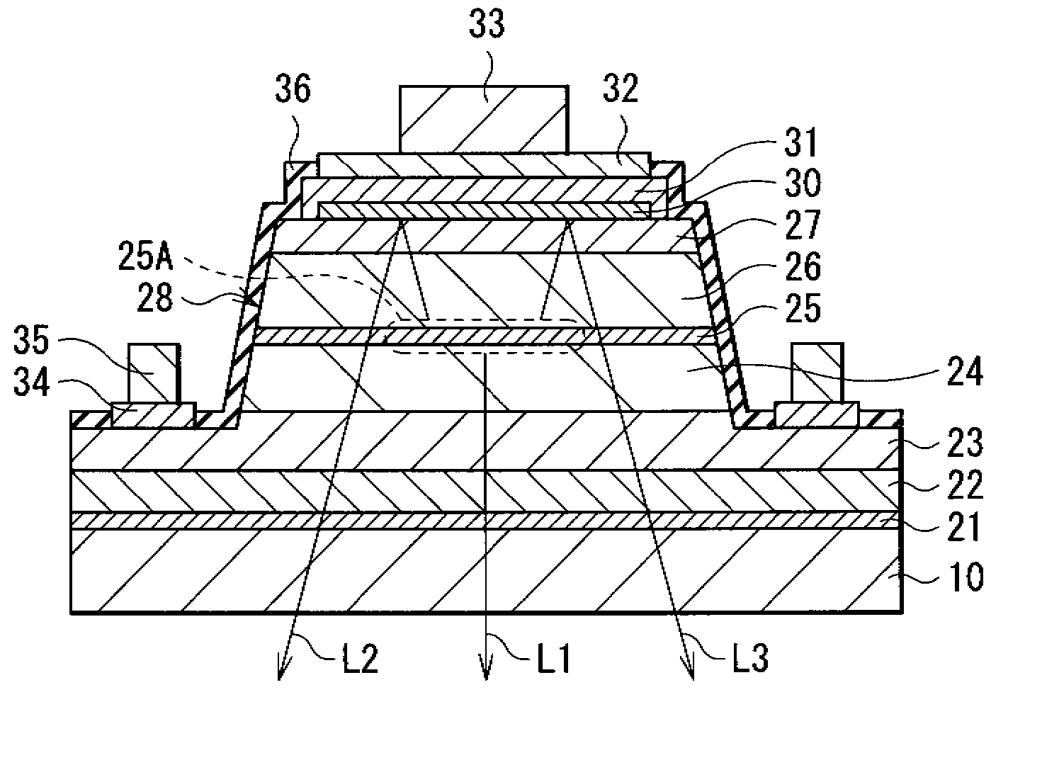
[0023]FIG. 1 shows a sectional view of a light emitting diode (LED) according to an embodiment of the invention. FIG. 1 is a schematic view, so dimensions and shapes in FIG. 1 are different from actual dimensions and shapes.

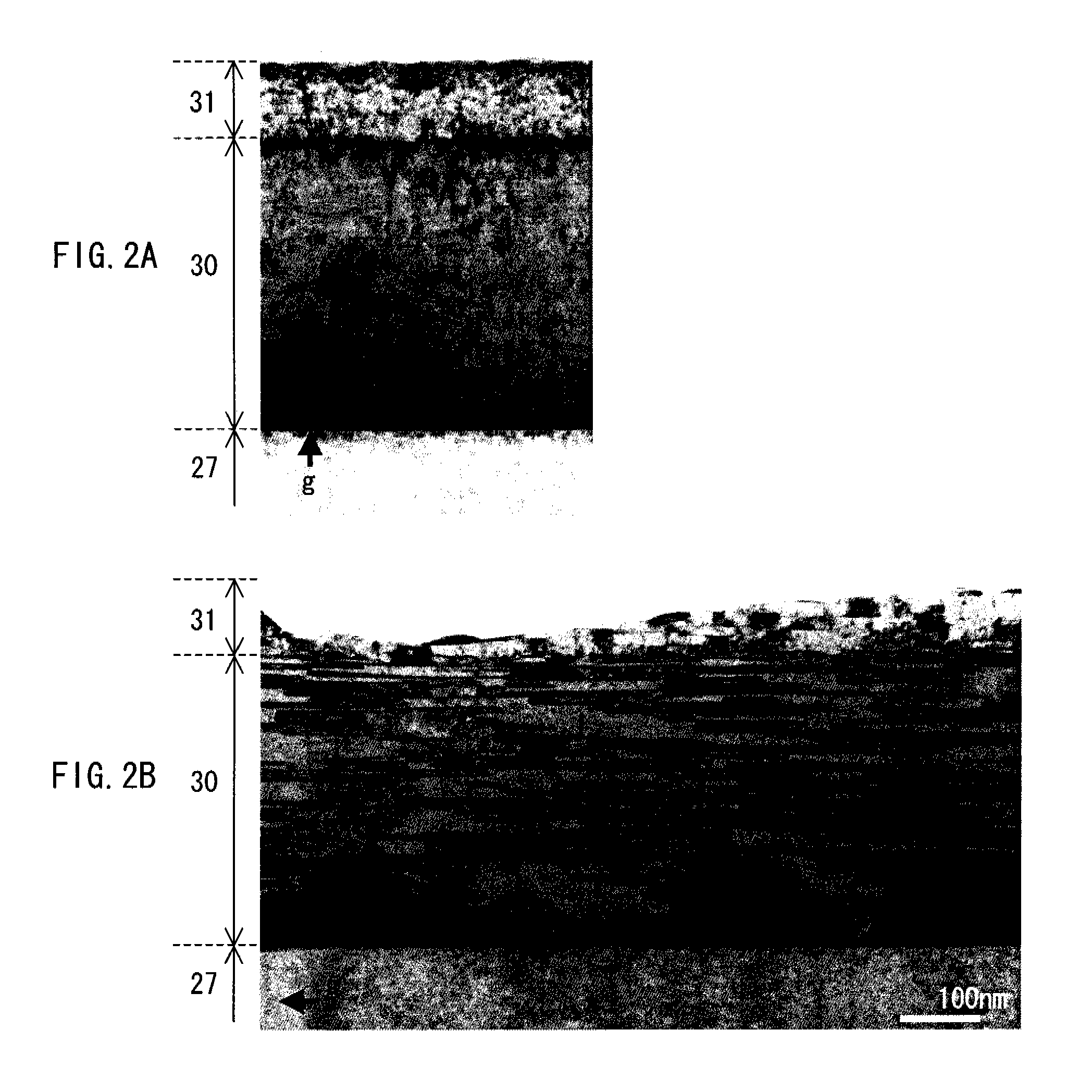
[0024] The light emitting diode is formed by growing a semiconductor layer 20 made of a nitride Group III-V compound semiconductor on a substrate 10. The semiconductor layer 20 is formed by laminating a buffer layer 21, a GaN layer 22, an n-type contact layer 23, an n-type cladding layer 24, an active layer 25, a p-type cladding layer 26 (a first p-type semiconductor layer) and a p-type contact layer 27 (a second p-type semiconductor layer) in this order.

[0025] The nitride Group III-V compound semiconductor here is a gallium nitride-based compound including gallium (Ga) and nitrogen (N), and examples of the gallium nitride-based compound include GaN, AlGaN (a...


PUM


Abstract

A semiconductor light emitting device having high reflectivity and a high electrical contact property between a light reflection layer and a semiconductor layer is provided. The semiconductor light emitting device is formed by laminating a semiconductor layer, a light reflection layer and a protective layer on a substrate in this order. The semiconductor layer is formed by laminating a buffer layer, a GaN layer, an n-type contact layer, an n-type cladding layer, an active layer, a p-type cladding layer and a p-type contact layer in this order. The light reflection layer is formed by depositing an Ag alloy on a surface of the p-type contact layer while heating the substrate at, for example, a temperature from 100° C. to less than 400° C. After the semiconductor layer, the light reflection layer and the protective layer are formed, the semiconductor layer, the light reflection layer and the protective layer are heated in a predetermined time range at an ambient temperature within a higher temperature range than a temperature range at the time of heating the substrate.

Description

CROSS REFERENCES TO RELATED APPLICATIONS [0001] The present invention contains subject matter related to Japanese Patent Application JP 2005-348294 filed in the Japanese Patent Office on Dec. 1, 2005, the entire contents of which being incorporated herein by reference. BACKGROUND OF THE INVENTION [0002] 1. Field of the Invention [0003] The present invention relates to a semiconductor light emitting device having a structure in which a light reflection layer reflects light emitted in a direction opposite to an emitting window toward the emitting window, and a method of manufacturing the semiconductor light emitting device. [0004] 2. Description of the Related Art [0005] The external quantum efficiency of semiconductor light emitting devices such as light emitting diodes (LEDs) includes two factors, that is, internal quantum efficiency and light extraction efficiency, and a semiconductor light emitting device with a long life, low power consumption and high power can be achieved by im...

Claims


Application Information

Patent Timeline
Patent Type & Authority Applications(United States)
IPC IPC(8): H01L33/00H01L21/00H01L33/10H01L33/12H01L33/20H01L33/32
CPCH01L33/32H01L33/405H01L33/44
Inventor WATANABE, YOSHIAKIHINO, TOMONORIKOBAYASHI, TOSHIMASANARUI, HIRONOBU
Owner SONY CORP
Why Eureka
Try Eureka