Imprint method, imprint apparatus, and process for producing chip

Active Publication Date: 2007-06-28
CANON KK
View PDF14 Cites 50 Cited by
  • Summary
  • Abstract
  • Description
  • Claims
  • Application Information

AI Technical Summary

Benefits of technology

[0037] According to the present invention, it is possible to realize a high throughput in

Problems solved by technology

Particularly, it has been pointed out that a step of filling the resin material in the spacing between the mold and the substrate is very time consuming.
For this reason, when the resin material flows in the space, a large resistance is

Method used


Image

  • Imprint method, imprint apparatus, and process for producing chip
  • Imprint method, imprint apparatus, and process for producing chip
  • Imprint method, imprint apparatus, and process for producing chip

Examples


first embodiment

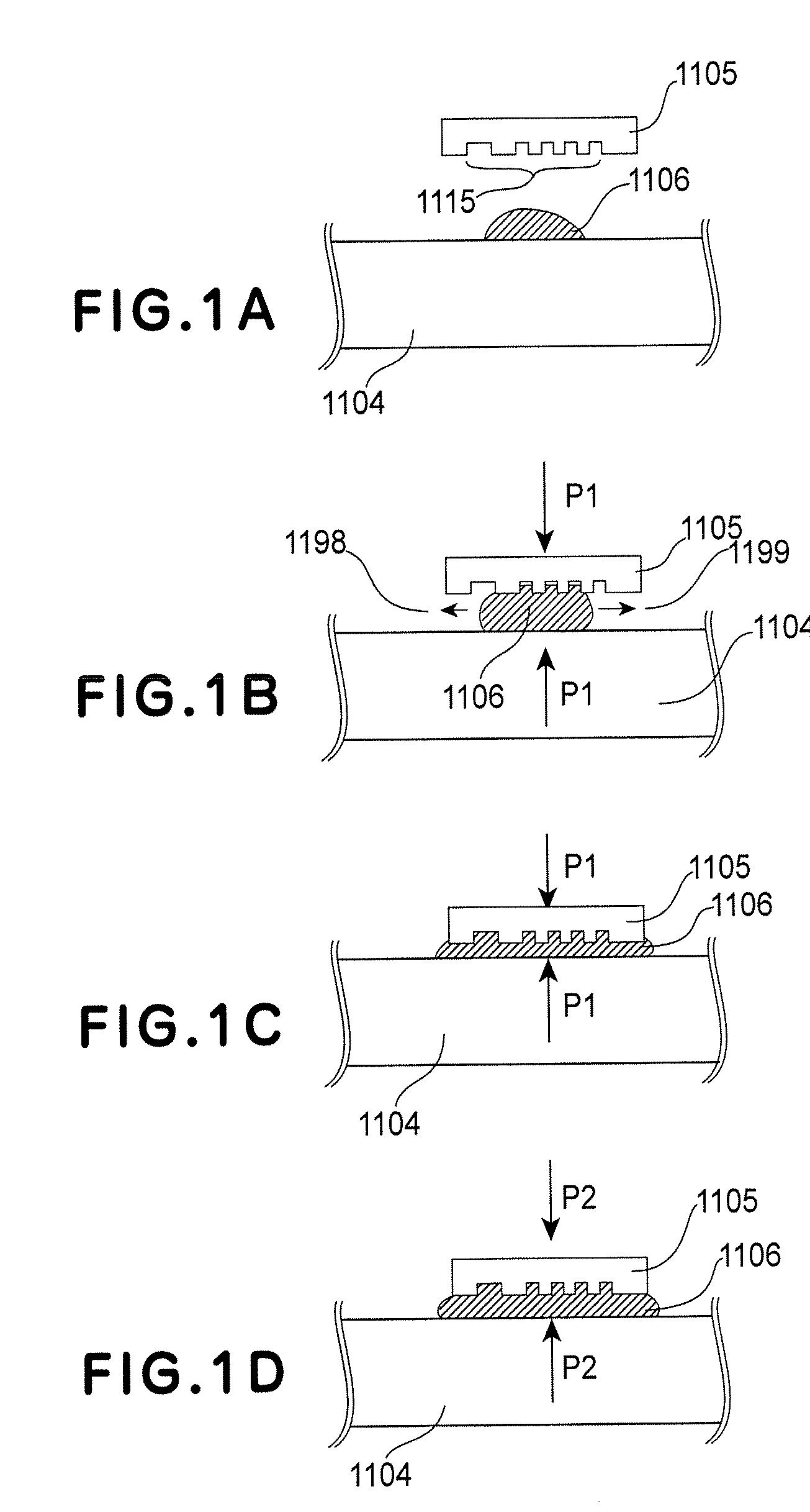
[0047] An imprint method according to First Embodiment of the present invention will be described with reference to FIGS. 1A to 1D.

[0048] Referring to FIG. 1A, a pattern formation material 1106 onto which an imprint pattern 1115 of a mold 1105 is imprinted is disposed on a substrate 1104. The mold 1105 and the substrate 1104 are disposed opposite to each other and a distance therebetween is gradually decreased, with the result that the mold 1105 and the pattern formation material 1106 contact each other.

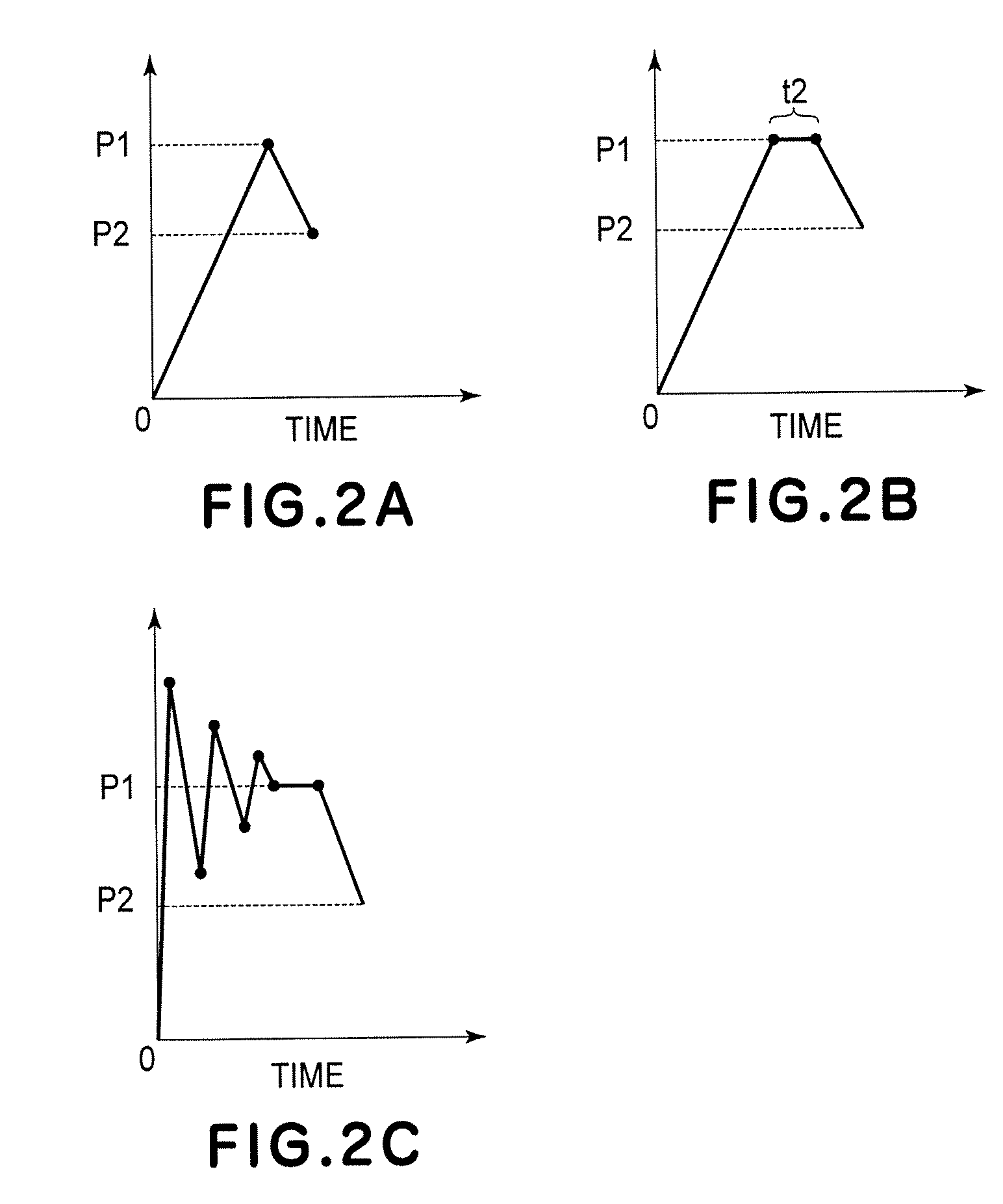
[0049] Thereafter, a pressure P1 is applied between the mold 1105 and the substrate 1104, whereby a contact area of the pattern formation material 1106 with the imprint pattern 1115 is increased (FIGS. 1B and 1C). In FIG. 1B, arrows 1198 and 1199 represent an example of directions in which the contact area is to be increased.

[0050] Incidentally, in this embodiment, the increase in contact area includes not only the case where the contact area is extended in an in-plane direction a...

second embodiment

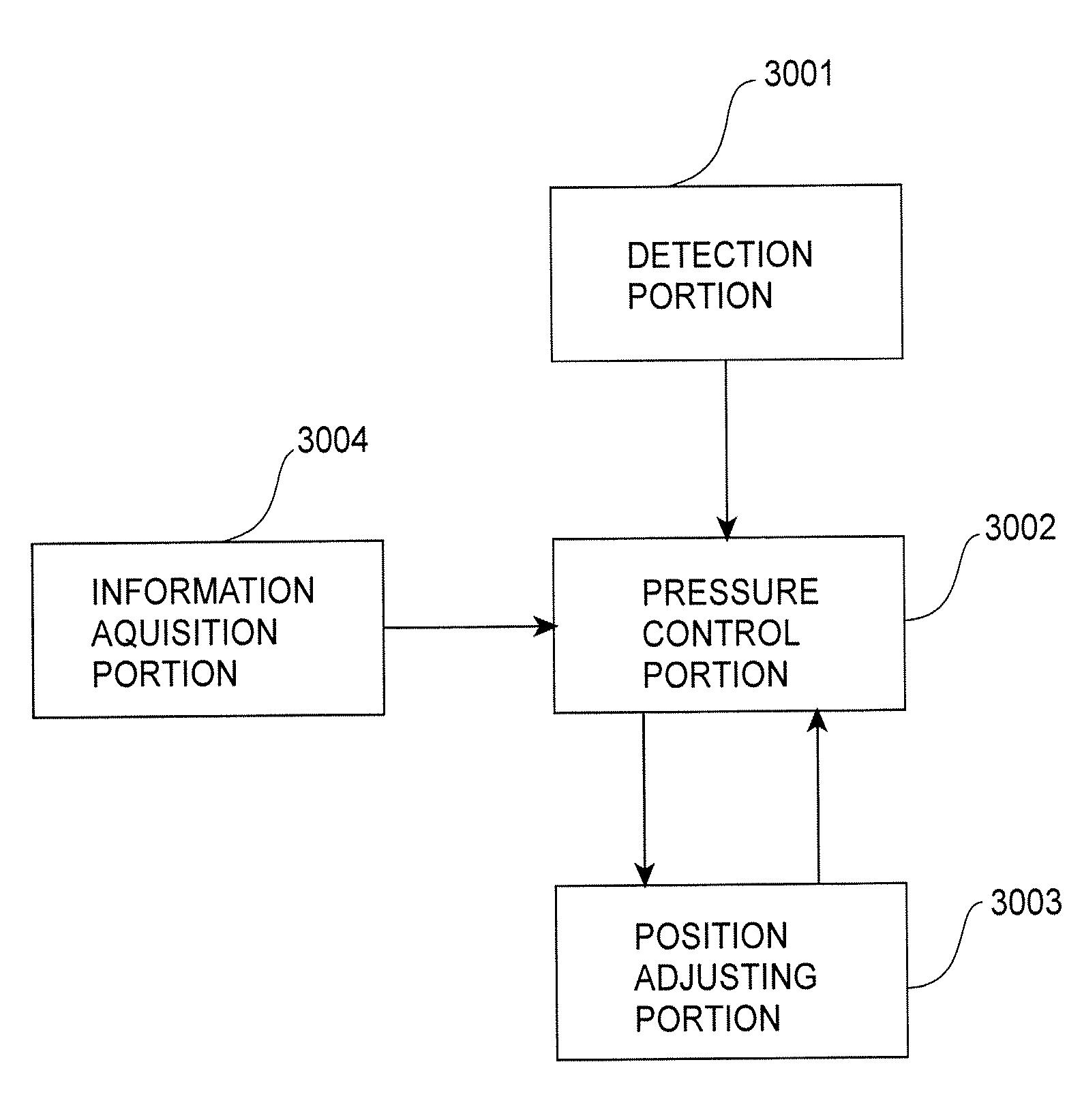
[0118] Next, the imprint apparatus according to Second Embodiment of the present invention will be described with reference to FIG. 3.

[0119] Herein, the imprint apparatus means such an imprint apparatus that the imprint pattern of the mold is imprinted onto the pattern formation material on the substrate and includes at least the following apparatus members or portions.

[0120] More specifically, the imprint apparatus includes a mold holding portion for holding the mold and a substrate stage for mounting thereon the substrate. The mold holding portion includes a chucking mechanism for chucking the mold.

[0121] The imprint apparatus further includes a detection portion 3001 for detecting the pressure or load exerted between the mold and the substrate, a pressure control portion 3002 for controlling the pressure exerted between the mold and the substrate, a position adjusting portion 3003 for adjusting the positional relationship between the mold and the substrate, and an information ...

third embodiment

Process

[0134] Next, a process for producing a chip according to Third Embodiment of the present invention will be described.

[0135] In the chip production process of this embodiment, as the imprint apparatus, it is possible to utilize the imprint apparatus used in Embodiments described later.

[0136] More specifically, the imprint pattern of the mold is imprinted onto the pattern formation material (e.g., the photocurable resin material). The photocurable resin material after the imprint pattern is imprinted thereon by energy irradiation with UV rays or the like ordinarily loses its photocurable property.

[0137] Thereafter, etching of the substrate (e.g., silicon substrate) is effected by using the pattern formation material as a mask.

[0138] Incidentally, it is also possible to remove a portion of the resin material at the recess formed on the resin material (herein, this portion is referred to as a “residual film”) by ashing (oxygen reactive etching), as desired, depending on the t...


PUM

PropertyMeasurementUnit
Pressureaaaaaaaaaa
Areaaaaaaaaaaa

Abstract

An imprint method for imprinting an imprint pattern of a mold onto a pattern formation material on a substrate so as to realize a high throughput includes the steps of bringing the imprint pattern and the pattern formation material into contact with each other; applying a first pressure between the mold and the substrate to increase a contact area between the imprint pattern and the pattern formation material; and adjusting a positional relationship between the mold and the substrate at a second pressure lower than the first pressure.

Description

FIELD OF THE INVENTION AND RELATED ART [0001] The present invention relates to an imprint method, an imprint apparatus, and a process for producing a chip by using the imprint apparatus. [0002] In recent years, e.g., as proposed in Appl. Phys. Lett., Vol. 67, Issue 21, pp. 3114-3116 (1995) by Stephan Y. Chou et al., fine processing technology for transferring a minute structure having an imprint pattern provided on a mold onto a work (or workpiece) such as a semiconductor, glass, resin or metal has been developed and has received attention. This technology is called nanoimprint or nanoembossing since it can be expected to realize a resolution on the order of several nanometers. Further, the nanoimprint technology is capable of forming a three-dimensional structure on a wafer at the same time, so that in addition to semiconductor fabrication technology, the technology has been expected to be applied to production technologies of optical devices such as photonic crystal, and productio...

Claims


Application Information

Patent Timeline
IPC IPC(8): B29C35/08B29C59/00B81C99/00
CPCB82Y10/00B82Y40/00G03F7/0002B41K3/02B81C1/0046B29C43/56
Inventor SEKI, JUNICHISUEHIRA, NOBUHITO
Owner CANON KK
Why Eureka
Try Eureka