Display apparatus

a technology of display apparatus and display screen, which is applied in the direction of instruments, static indicating devices, etc., can solve the problems of large shrinkage of glass substrate itself, low alignment accuracy, and large area, so as to reduce the frame size of the substrate, reduce the width of an area, and reduce the layout area

Inactive Publication Date: 2007-06-28
CANON KK
View PDF4 Cites 20 Cited by
  • Summary
  • Abstract
  • Description
  • Claims
  • Application Information

AI Technical Summary

Benefits of technology

[0019] According to the display apparatus of the present invention, a layout area is capable of being reduced by decreasing a width of an area, in which an amount of current in a common interconnecting line, disposed to surround an area in which a plurality of constituents each including a current drive-type light-emitting device and a device control circuit. As a result, it is possible to reduce a frame size of the substrate. Further, by the wiring design in view of current path, a width of the common interconnecting line on a side where a drive circuit for driving the device control circuit is disposed is decreased, so that it is possible to suppress an increase in frame size resulting from an increase in circuit area. Thus, it is possible to provide a display apparatus capable of alleviating the increase in frame size in order to realize an apparatus of light weight and compact.

Problems solved by technology

However, the glass substrate is large, so that the glass substrate itself has a large shrinkage.
As a result, alignment accuracy is approximately 1 μm, thus being not high.
Further, it is difficult to form respective metal layer patterns at a processing accuracy of 2 μm or less by a currently available large-size pattern processing apparatus (etching apparatus etc.).
As described above, it is not easy to provide the peripheral circuit or signal processing circuit with high resolution from the viewpoints of production such as the alignment accuracy and the processing accuracy.
In an organic EL panel, when moisture permeates an organic EL device, an associated pixel results in a defective dot.
In addition, adjacent pixels of the moisture-permeated pixel are successively adversely affected by the moisture-permeated pixel to increase a dark spot as a non-luminous area.
Finally, the entire display panel cannot effect display.
As a result, there is a possibility that the defective pixel is increased, thus causing a deterioration in display state.
As a result, at either side, a wide frame area is required, so that it is more difficult to reduce the frame area of the display panel.

Method used


Image

  • Display apparatus
  • Display apparatus
  • Display apparatus

Examples


embodiment 1

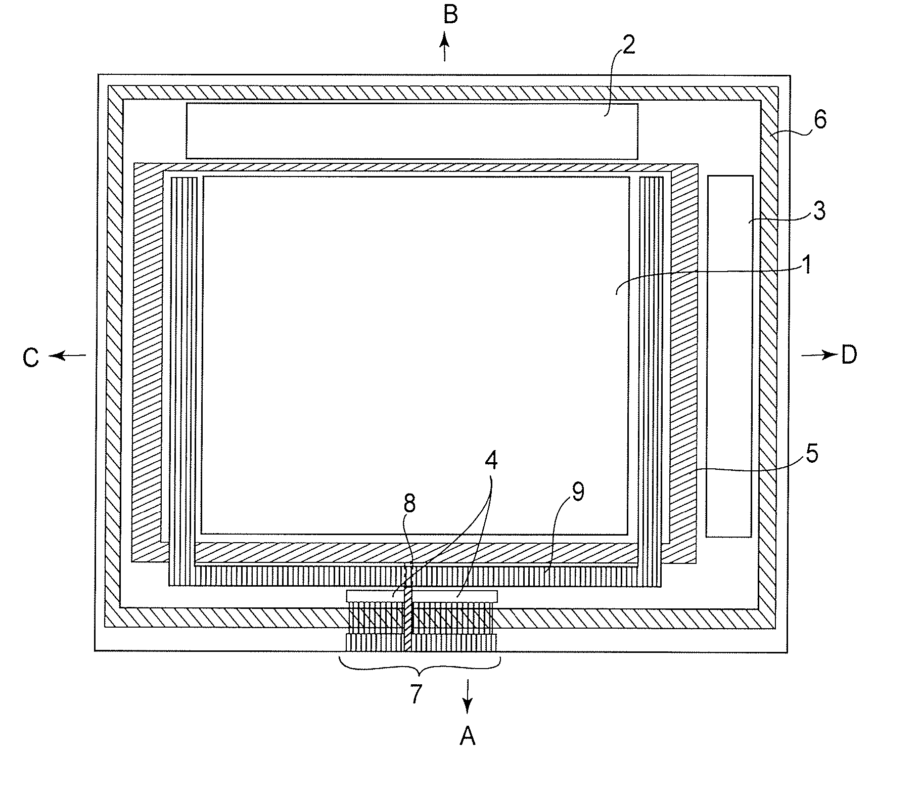
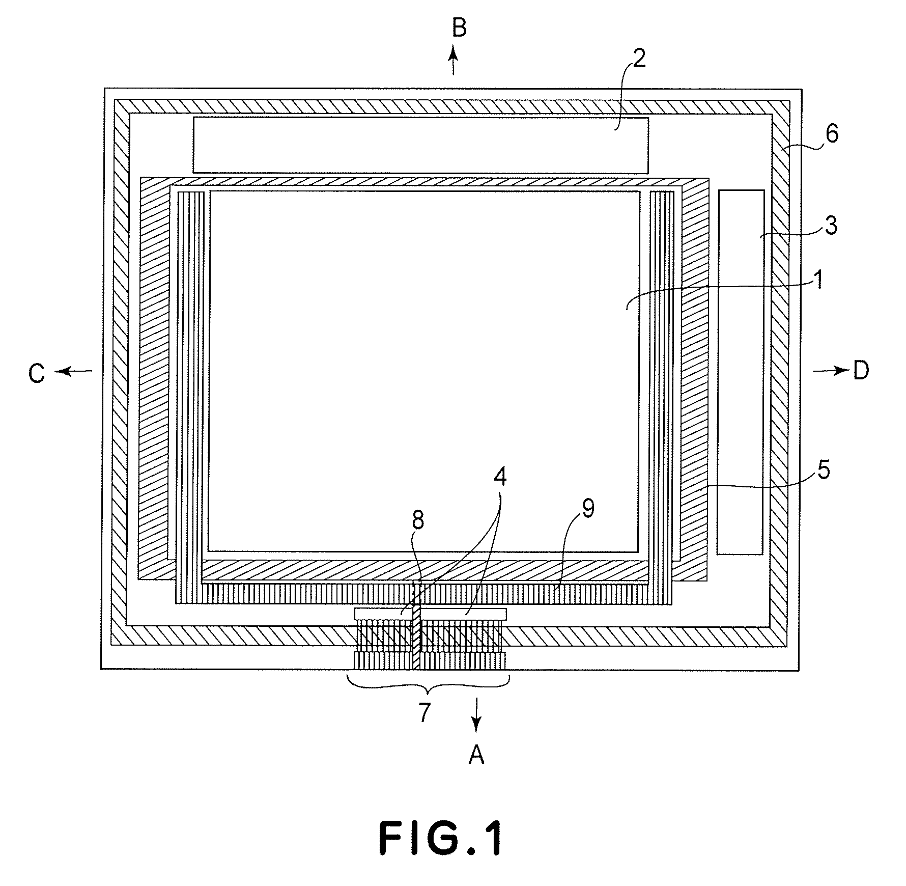
[0035]FIG. 1 is a schematic layout view of a display apparatus according to Embodiment 1 of the present invention.

[0036] The display apparatus shown in FIG. 1 includes a display area 1 in which pixels (constituents) each comprising an EL device such as an organic EL device or the like and a pixel circuit (device control circuit) including a thin film transistor (TFT) are arranged in a matrix.

[0037] The display apparatus further includes a data line drive circuit 2 for outputting a data signal to data lines electrically connected to associated pixel columns, respectively, a scanning line drive circuit 3 for outputting a scanning signal to scanning liens electrically connected to associated pixel rows, respectively, a terminal portion 7 for inputting an image signal or a control signal and supplying electric power, an input circuit 4 for converting the inputted control signal into an operation voltage level in a display panel, an adhesive area 6 for effecting adhesion of a sealing s...

embodiment 2

[0057]FIG. 5 is a schematic layout view of a display apparatus according to Embodiment 2 of the present invention.

[0058] In this embodiment, a side of a display area 11 most distant from the lead-out portion 8 is parallel to a signal line. Between the side and an edge of the substrate close to the side, a scanning line drive circuit is disposed.

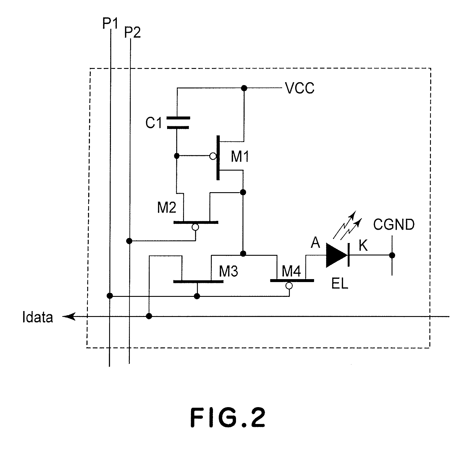
[0059] The display apparatus shown in FIG. 5 includes a display area 11 in which pixels (constituents) each comprising an EL device and a pixel circuit (device control circuit) including a thin film transistor (TFT) are arranged in a matrix. A constitution of the pixel is identical to that shown in FIG. 2. Similarly, those of pixels in Embodiments described later are also identical to that shown in FIG. 2.

[0060] The display apparatus further includes a data line drive circuit 12 for outputting a data signal to data lines electrically connected to associated pixel columns, respectively, a scanning line drive circuit 13 for outputting a scan...

embodiment 3

[0064]FIG. 6 is a schematic layout view of a display apparatus according to Embodiment 3 of the present invention.

[0065] A difference of this embodiment shown in FIG. 6 from Embodiment 1 shown in FIG. 1 is that a common interconnecting line 5 on a side B located opposite, via the display area 1, from the wiring lead-out portion 8 is interrupted, thus being not a continuous rectangular shape.

[0066] As in this case, even when the common interconnecting line 5 on the side B is partially cut off and fails to establish a continuous connection state, an amount of current flowing toward the side B is smaller than those of current flowing toward the sides A, C and D. For this reason, the influence of the cutting-off of the common interconnecting line 5 is small.


PUM

PropertyMeasurementUnit
areaaaaaaaaaaa
widthaaaaaaaaaa
electroluminescenceaaaaaaaaaa

Abstract

A display apparatus includes, on a substrate, an area in which a plurality of constituents each including a light-emitting device and a device control circuit for controlling current passing through the light-emitting device is disposed, a common interconnecting line disposed to surround a periphery of the area, a terminal portion for permitting electrical connection to an external circuit, and a wiring lead-out portion for electrically connecting the common interconnecting line to the terminal portion. The light-emitting device is disposed, on the substrate, between a lower first electrode and an upper second electrode. The first electrode is electrically connected to the device control circuit, and the second electrode is electrically connected to the common interconnecting line through a contact hole. The common interconnecting line disposed along a side of the area most distant from the wiring lead-out portion has a narrower width than a width of the common interconnecting line disposed along a side of the area closer to the wiring lead-out portion.

Description

FIELD OF THE INVENTION AND RELATED ART [0001] The present invention relates to a current drive-type display apparatus having an area in which a plurality of constituents each including a current drive-type light-emitting device and a device control circuit for controlling current passing through the light-emitting device is disposed on a substrate, and relates to a camera including the display apparatus. The present invention is suitably used in a display apparatus using an electroluminescence (EL) device which produces luminescence by injecting current therein. [0002] A display panel applied to a lightweight and compact apparatus requires a small substrate size and a sufficiently large display area. For this reason, it is desirable that a peripheral area of the display area, i.e., a frame area is as small as possible. In the frame area, a peripheral circuit or a signal processing circuit, an interconnecting line for supplying electric power, and in the case of using a sealing subst...

Claims


Application Information

Patent Timeline
Patent Type & Authority Applications(United States)
IPC IPC(8): G09G3/30
CPCG09G3/325G09G2300/0426G09G2300/0842G09G2300/0861
Inventor GODEN, TATSUHITOKAWASAKI, SOMEIISEKI, MASAMI
Owner CANON KK
Why Eureka
Try Eureka