

Manufacture method for ZnO based compound semiconductor crystal and ZnO based compound semiconductor substrate
- Summary
- Abstract
- Description
- Claims
- Application Information
AI Technical Summary
Benefits of technology
Problems solved by technology
Method used
Image

Examples
Embodiment Construction
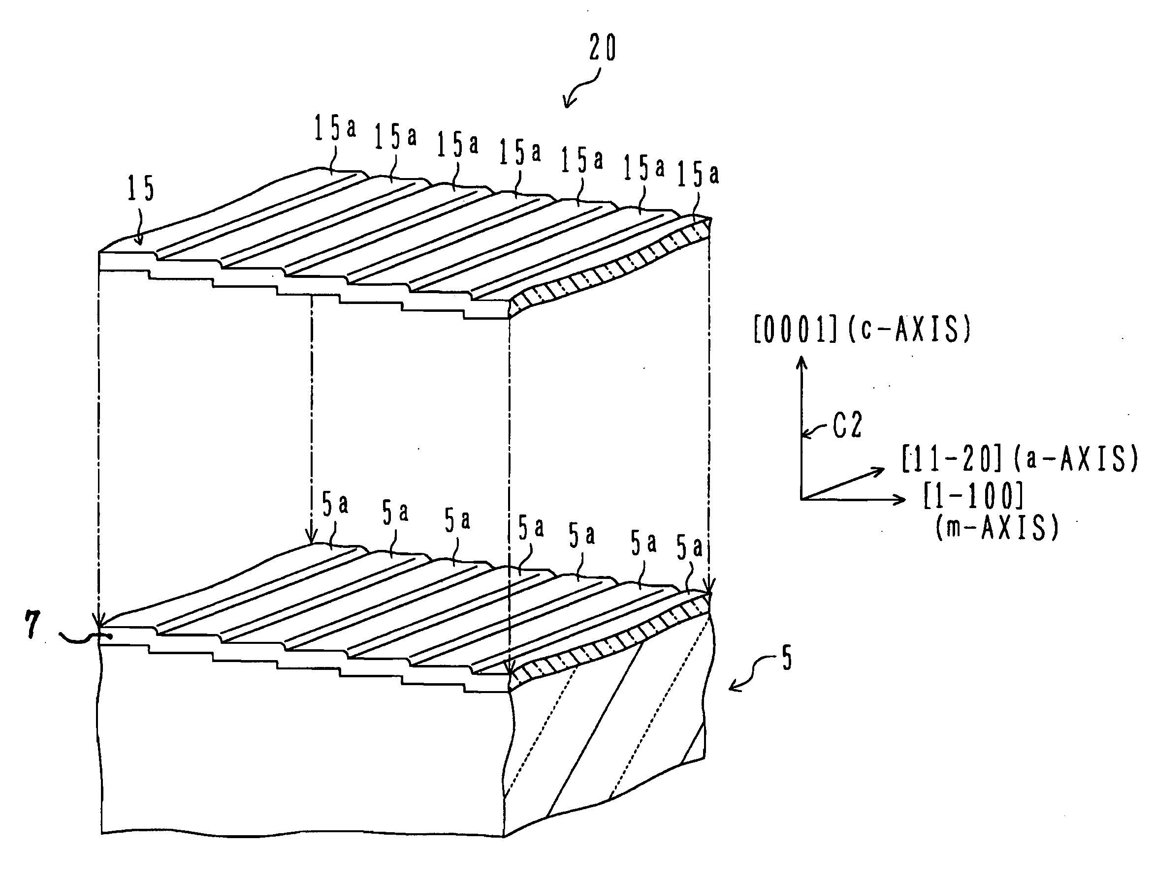
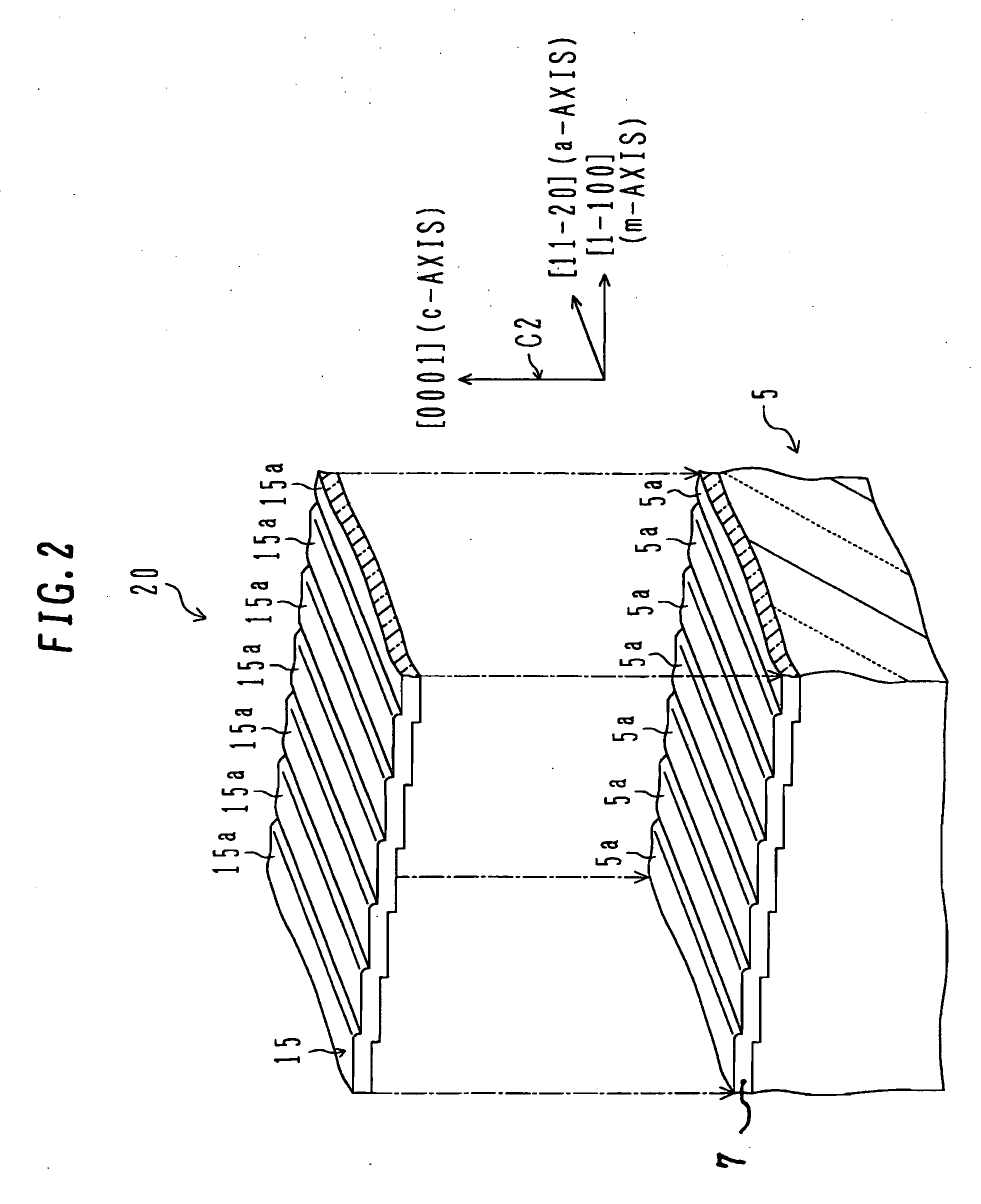
[0028] With reference to FIGS. 1 and 2, a manufacture method for ZnO based compound semiconductor crystal according to an embodiment of the present invention is described.
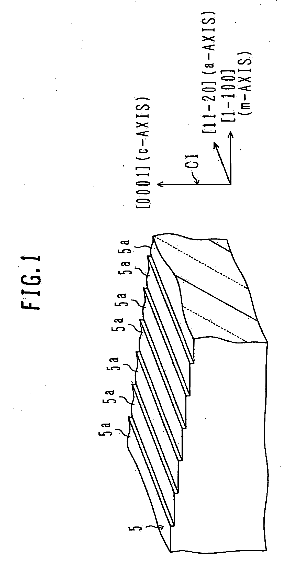
[0029]FIG. 1 is a schematic perspective view showing a crystal growth substrate 5 for growing ZnO based compound semiconductor crystal according to the embodiment.
[0030] The crystal growth substrate 5 is made of ZnO single crystal having a hexagonal system Wurtzite structure. In FIG. 1 (and FIG. 2), a coordinate system C1 showing the directions of crystal axes (a-axis, c-axis and m-axis) of the crystal growth substrate 5 is shown. In the coordinate system C1, the a-, c- and m-axes cross at a right angle, the c-axis being represented by Miller indices [0001], the m-axis being represented by Miller indices [1-100] and the a-axis being represented by Miller indices [11-20]. Although a negative value is represented by adding a “bar” over a numerical value according to the usual coding scheme of Miller index, in the p...
PUM
| Property | Measurement | Unit |
|---|---|---|
| Angle | aaaaa | aaaaa |
| Angle | aaaaa | aaaaa |
| Angle | aaaaa | aaaaa |
Abstract
Description
Claims
Application Information