Method for measuring an amount of strain of a bonded strained wafer

a strain measurement and strain measurement technology, applied in the direction of individual semiconductor device testing, semiconductor/solid-state device testing/measurement, instruments, etc., can solve the problem of inability to obtain inability to separate and measure the amount of strain, and inability to achieve accurate strain strain of strained si layer. the effect of tim

Active Publication Date: 2007-07-19
SHIN-ETSU HANDOTAI CO LTD
View PDF3 Cites 12 Cited by
  • Summary
  • Abstract
  • Description
  • Claims
  • Application Information

AI Technical Summary

Benefits of technology

[0016] Accordingly, the present invention was conceived in view of the above problems. An object of the present invention is to provide a method for measuring an amount of strain by which amounts of strain in the horizontal direction and in the vertical direction of the strained layer in a bonded strained wafer can be measured by the X-ray diffraction method in a shorter time and more simply.
[0020] As described above, when the amount of strain of the strained layer is calculated, in the case that two peaks for the respective diffraction planes of the single crystal substrate appearing on the reciprocal lattice space map are located at symmetric positions with respect to a vertical axis passing through the origin of the reciprocal lattice space map, the axis setting has accurately been conducted at measuring respective diffraction planes. Therefore, the peak positions for the strained layer are moved rotationally and modified in the circumferential direction centering the origin so that the two peak positions for the respective diffraction planes of the same strained layer appearing on the reciprocal lattice space map is located symmetrically with respect to the vertical axis, and thereby the peak positions for the strained layer determined by the amount of strain can be obtained with removing effect of crystal orientation declination due to Tilt, Twist, or the like.
[0030] Because peak positions for the SiGe layer in which the lattice relaxation rate becomes 0% and 100% can be easily calculated from the rotated and modified peak positions for the SiGe layer, the respective lattice relaxation rates in the horizontal direction and in the vertical direction can be calculated easily from the relation of these calculated peak positions.
[0032] Because a lattice constant of the strained silicon layer can be calculated easily from the rotated and modified peak positions for the strained silicon layer, the respective strain rates in the horizontal direction and in the vertical direction can be calculated easily from the lattice constant thus calculated and from the normal lattice constant of silicon.
[0033] According to the present invention, amounts of strain in the horizontal direction and in the vertical direction can be easily measured in the reciprocal lattice space map obtained from two asymmetric diffraction planes according to X-ray diffraction method. Moreover, measurement of a Tilt angle and a Twist angle are not required in addition, and measurement according to an X-ray diffraction method for creating a reciprocal lattice space map can be accomplished only at the two diffractions of (XYZ) and (−X−YZ). Therefore, measuring can be done in a shorter time and more simply.

Problems solved by technology
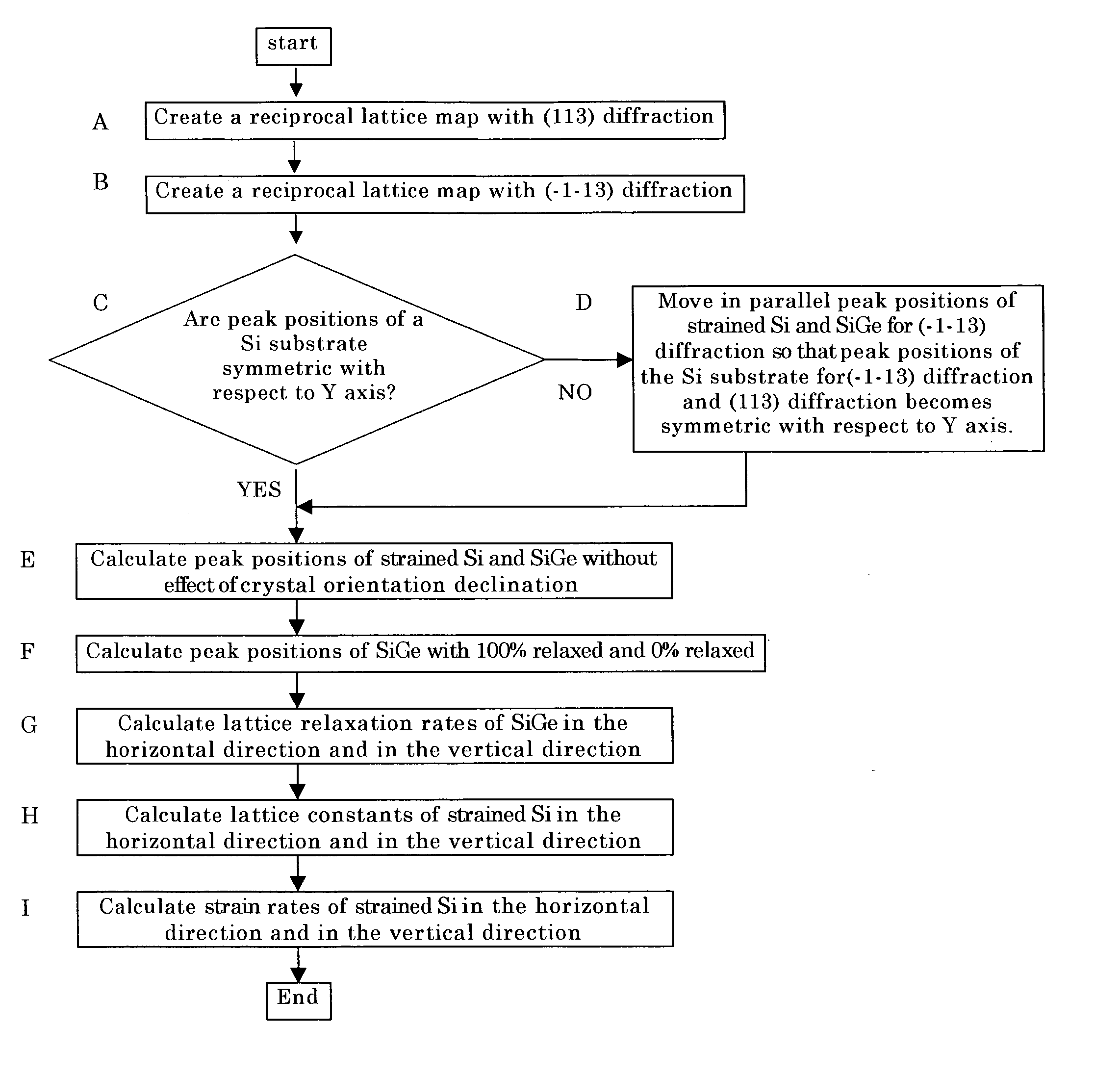
However, for example, in the case of SSOI (Strained Silicon On Insulator) structure formed using two Si substrates by a bonding method as described in the documents, an accurate lattice relaxation rate (or a strained rate) has not been possible to be obtained.
Therefore, only an amount of strain cannot be separated and measured and an accurate amount of strain of the strained Si layer cannot be obtained.
Therefore, carrier mobility of the produced strained Si layer cannot be evaluated accurately.
However, in this method, measurement of a Tilt angle and a Twist angle is required to be performed in addition, and measurement of a reciprocal lattice space map taking about 8 hours in one time is required to be performed 4 times at intervals of 90°, therefore there is a problem that an extremely long time has to be used on evaluation of a strain rate (a lattice relaxation rate).
However, in this method, there is a problem that only an amount of strain in the horizontal (plane) direction can be measured and an amount of strain in the vertical (depth) direction cannot be measured.
Moreover, there is a problem that in the case of measuring a lattice relaxation rate of the SiGe layer by micro-Raman spectroscopy, it cannot be measured unless a Ge concentration in the SiGe layer is preliminarily given.
However, because this is fundamentally a destructive inspection, there is a problem that this method reduces yield of wafers in production.

Method used


Image

  • Method for measuring an amount of strain of a bonded strained wafer
  • Method for measuring an amount of strain of a bonded strained wafer
  • Method for measuring an amount of strain of a bonded strained wafer

Examples


experiment 1

(Experiment 1)

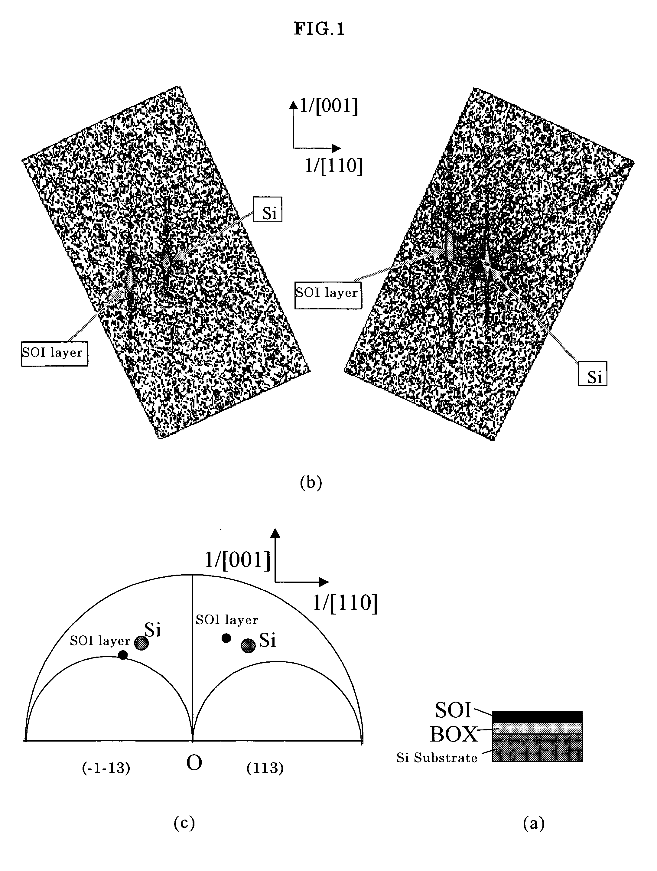
[0050] By using two silicon single crystal wafers with a 200 mm diameter, p-type, and crystal orientation of , there is prepared a bonded SOI wafer based on a Si substrate which has a 110-nm thickness of an SOI layer and a 200-nm thickness of a buried oxide film layer (Buried Oxide, hereinafter, referred to as a BOX layer) and which is produced according to smart cut (a registered trademark) method. And measurement of a reciprocal lattice space map of a (113) diffraction plane and a (−1−13) diffraction plane was performed by an X-ray diffraction apparatus (manufactured by Philips Co. Ltd.).

[0051]FIG. 1(a) is a section schematic view of the measured SOI wafer. (b) is a reciprocal lattice space map thereof. (c) is a schematic view showing diffraction strength peak positions on the reciprocal lattice space map. In addition, in the reciprocal lattice space map, an axis in the horizontal direction is 1 / [110], an axis in the vertical direction is 1 / [001]. From the reciproca...

experiment 2

(Experiment 2)

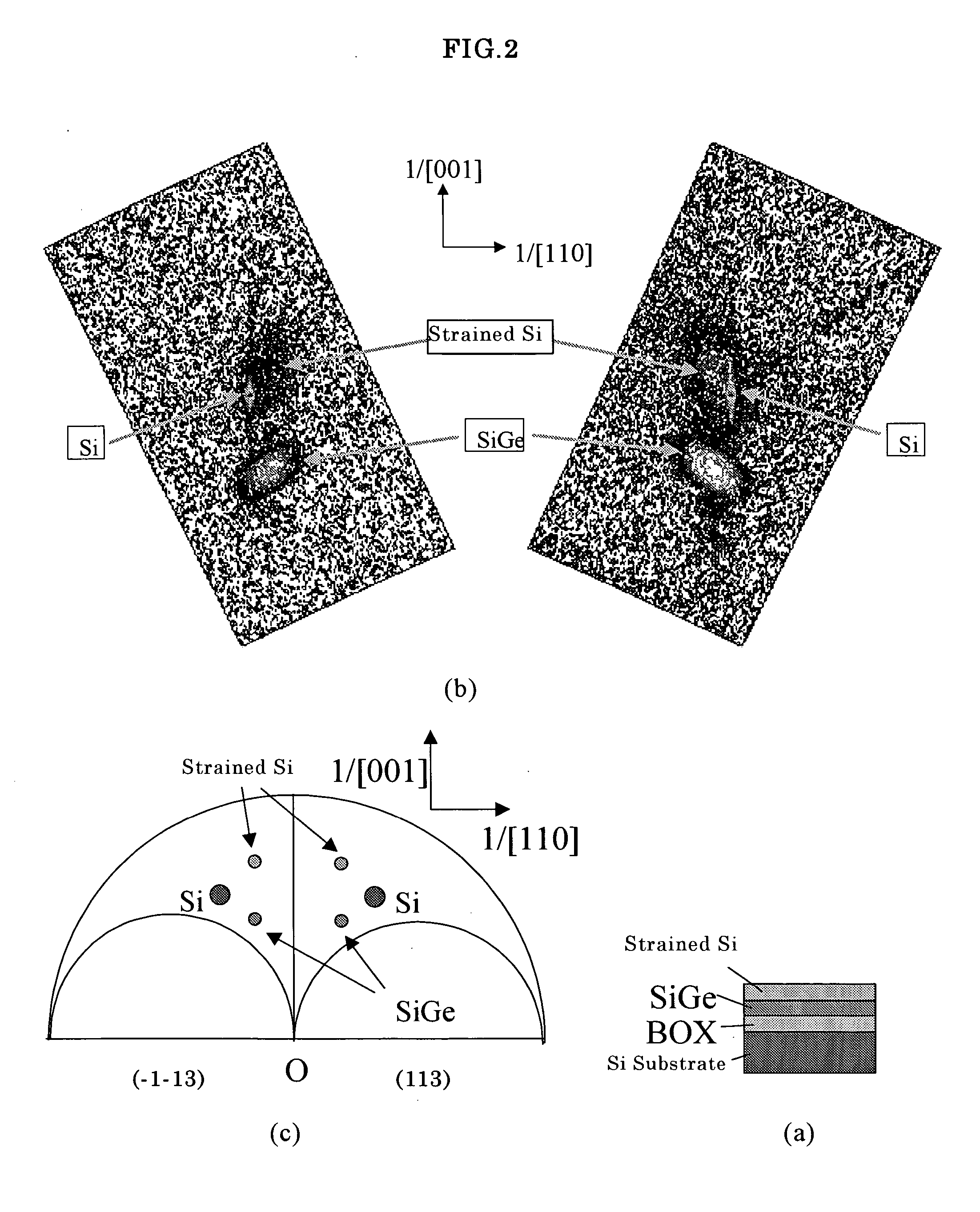
[0055] By using silicon single crystal wafers with a 200 mm diameter, p-type, and crystal orientation of , an SGOI wafer (strained Si / SiGe / BOX / Si substrate) with a 20% Ge concentration of a SiGe layer, a 40-nm thickness of the SiGe layer, and a 150-nm thickness of a BOX layer was produced according to a SIMOX method and an oxidation-concentration method. And measurement of reciprocal lattice space maps of a (113) diffraction plane and a (−1−13) diffraction plane was performed with X-ray diffraction apparatus in the same manner as Experiment 1.

[0056]FIG. 2(a) is a section schematic view of an SGOI wafer. (b) is a reciprocal lattice space map thereof. (c) is a schematic view showing peak positions on the reciprocal lattice space map. In addition, an axis in the horizontal direction of the reciprocal space map is 1 / [110], an axis in the vertical direction thereof is 1 / [001]. From the reciprocal lattice space map, peak positions for the SiGe layer and peak positions for t...

example 1

[0083] As a sample 1 for measuring a lattice relaxation rate of a SiGe layer, production of an SGOI wafer using the oxidation-concentration method was performed. On a bonded SOI wafer with a 200-mm diameter produced by smart cut (a registered trademark) method, a SiGe layer was produced at a 20-% Ge concentration at a 40-nm thickness, and then Ge was diffused into the SOI layer by performing dry-oxidation at a temperature of 1000° C. or more, and therewith the SOI layer (which becomes a SiGe layer after the oxidation-concentration step) was thinned, then an oxide film on its surface is removed by using a HF solution, and thereby forming a SiGe layer with a 20-% Ge concentration and a 40-nm thickness on a BOX layer. At this time, the object was to measure a lattice relaxation rate of the SiGe layer, therefore, a strained Si layer was not formed on the SiGe layer.

[0084] And, measurement of a reciprocal lattice space map of a (113) diffraction plane and a (−1−13) diffraction plane was...


PUM

PropertyMeasurementUnit
thicknessaaaaaaaaaa
temperatureaaaaaaaaaa
thicknessaaaaaaaaaa

Abstract

The present invention is a method for measuring an amount of strain of a bonded strained wafer in which at least one strained layer is formed on a single crystal substrate by a bonding method, wherein at least, the bonded strained wafer is measured with respect to two asymmetric diffraction planes with diffraction plane indices (XYZ) and (−X−YZ) by an X-ray diffraction method, a reciprocal lattice space map is created from the measured data, and the amount of strain of the strained layer is calculated from the peak positions for the respective diffraction planes of the single crystal substrate and the strained layer appearing on the reciprocal lattice space map. Thereby, there can be provided a method for measuring an amount of strain by which amounts of strain in the horizontal direction and in the vertical direction of the strained layer by an X-ray diffraction method in a bonded strained wafer can be measured in a shorter time and more simply.

Description

TECHNICAL FIELD [0001] The present invention relates to a method for measuring an amount of strain of a bonded strained wafer in which at least one strained layer is formed on a single crystal substrate by a bonding method. Background Art [0002] A so-called strained Si layer which is a thin-film silicon (Si) single crystal layer to which tensile strain is introduced has attracted attention as material for satisfying demands for high-speed semiconductor devices in recent years because high carrier mobility can be obtained as compared to a normal Si layer with no strain. [0003] The strained Si layer can be obtained, for example, by forming a SiGe layer by epitaxial growth on a Si substrate with crystal plane orientation of (100), furthermore epitaxially growing a Si layer on the SiGe layer, thereby introducing tensile strain to the Si layer by utilizing the characteristic that a lattice constant of the SiGe layer is a little larger than a lattice constant of the Si layer. At this time...

Claims


Application Information

Patent Timeline
Patent Type & Authority Applications(United States)
IPC IPC(8): H01L21/66G01N23/207H01L21/02H01L21/20H01L21/762H01L27/12
CPCG01N23/207H01L21/76251G01N2223/6116G01N2223/607
Inventor YOKOKAWA, ISAO
Owner SHIN-ETSU HANDOTAI CO LTD
Why Eureka
Try Eureka