Methods and Apparatuses for Manufacturing Monocrystalline Cast Silicon and Monocrystalline Cast Silicon Bodies for Photovoltaics

Inactive Publication Date: 2007-07-26
THE UNITED STATES AS REPRESENTED BY THE DEPARTMENT OF ENERGY +1
View PDF86 Cites 102 Cited by
  • Summary
  • Abstract
  • Description
  • Claims
  • Application Information

AI Technical Summary

Benefits of technology

[0011]As used herein, the term “monocrystalline silicon” refers to a body of single crystal silicon, having one consistent crystal orientation throughout. Further, convention

Problems solved by technology

Monocrystalline silicon is, however, more expensive to produce than conventional multi-crystalline silicon, using known techniques such as those described above.
The random orientation of grains, in either conventional multi-crystalline or poly-crystalline silicon, makes it difficult to texture the surface of a resulting wafer.
Additionally, “kinks” that form in the boundaries between the grains of conventional multi-crystalline silicon tend to nucleate structural defects in the form of clusters or lines of dislocations.
This can cause a decrease in the efficiency of the cell.
Photovoltaic

Method used


Image

  • Methods and Apparatuses for Manufacturing Monocrystalline Cast Silicon and Monocrystalline Cast Silicon Bodies for Photovoltaics
  • Methods and Apparatuses for Manufacturing Monocrystalline Cast Silicon and Monocrystalline Cast Silicon Bodies for Photovoltaics
  • Methods and Apparatuses for Manufacturing Monocrystalline Cast Silicon and Monocrystalline Cast Silicon Bodies for Photovoltaics

Examples


example 1

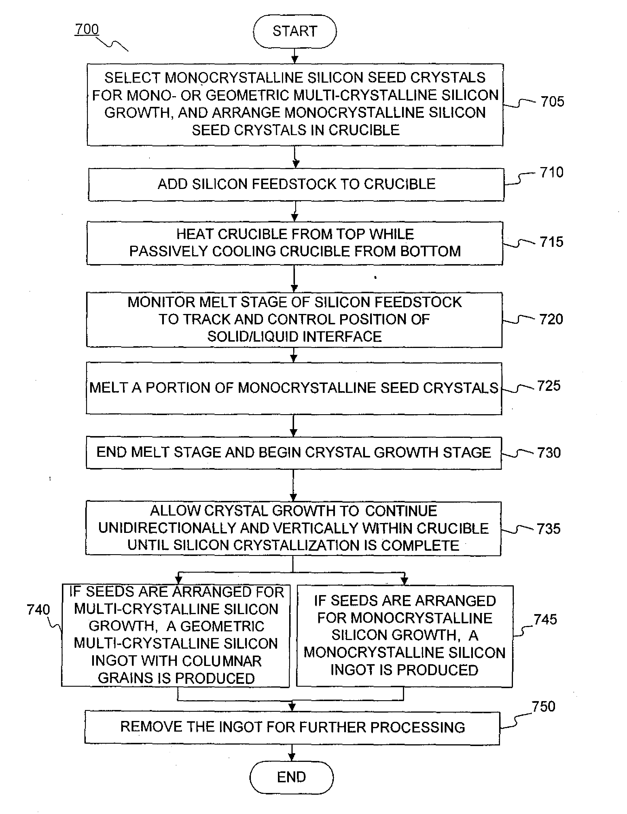
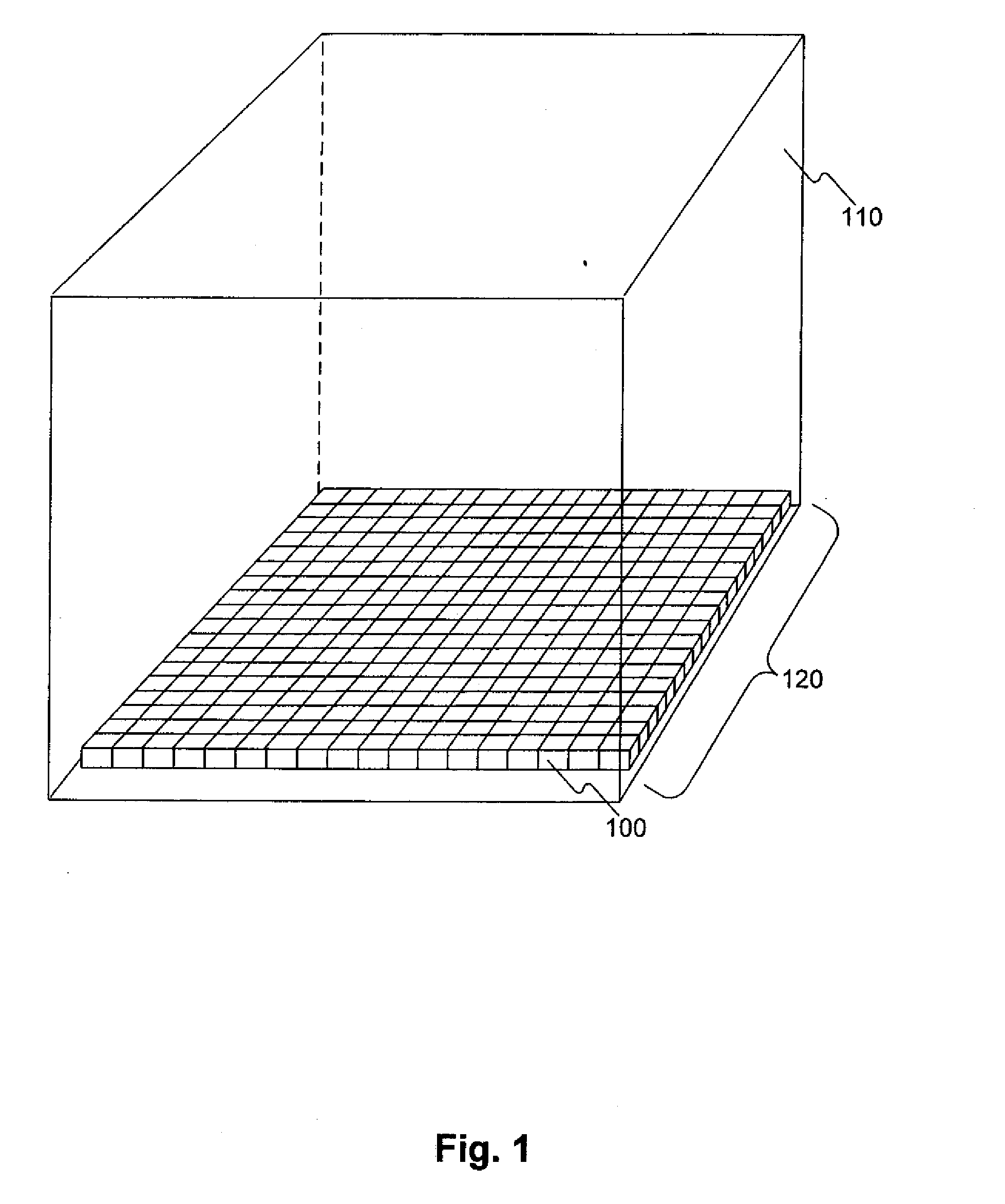
[0101]Seed preparation: A boule of pure Czochralski (CZ) silicon (monocrystalline), obtained from MEMC, Inc. and having 0.3 ppma of boron, was cut down along its length using a diamond coated band saw so that it had a square cross section measuring from 14 cm per side. The resulting block of monocrystalline silicon was cut through its cross section using the same saw into slabs having a thickness of about 2 cm to about 3 cm. These slabs were used as monocrystalline silicon seed crystals, or “seeds.” The (100) crystallographic pole orientation of the silicon boule was maintained. The resulting single crystal silicon slabs were then arranged in the bottom of a quartz crucible so that the (100) direction of the slabs faced up, and the (110) direction was kept parallel to one side of the crucible. The quartz crucible had a square cross section with 68 cm on a side, a depth of about 40 cm, and a wall thickness of about 1.8 cm. The slabs were arranged in the bottom of the crucible with th...

example 2

[0104]Seed preparation: Seeding was accomplished as in Example 1, except that the monocrystalline silicon seeds were cut so that the (110) direction was at 45 degrees from the side of the square seeds for half of the seeds, while the other half had an angle of approximately 20 degrees. The square pieces were layered in the bottom of the crucible in a checkerboard manner alternating the two different seed orientations, i.e., the (110) direction had an angle of 45 degrees and 20 degrees from the orientation of the crucible sides. Relative to one another, the seeds had either 25 degrees or 155 degrees of misorientation. However, due to size mismatches of the square-shaped seeds, some gaps in the seeding layer were left uncovered. The crucible measured approximately 33 cm on each of the square sides and approximately 22 cm tall.

[0105]Casting: The crucible containing the seeds and a separate crucible containing a total of 56 kg of feedstock silicon chunks were loaded into a Ubiquitous Ca...

example 3

[0106]Seed preparation: Seeding was accomplished with 23 kg of square, (100), plates used to line the bottom of a crucible, providing a coverage area of 63 cm×63 cm and a thickness ranging from 3 cm in the center to 1.8 cm at the sides. All plates were arranged with their (110) directions at 45° from the walls of the crucible.

[0107]Casting: The crucible containing the seeds was filled with an additional total of 242 kg of feedstock silicon chunks, representing a mix of intrinsic silicon, silicon recycled from previous ingots, and double-cast silicon with a p-type resistivity greater than 9 ohm-cm. The charge of silicon in the crucible was loaded into a one-stage directional solidification furnace. The crucible (with the seeds inside) was heated up to a temperature of 1550° C., while the bottom was cooled by opening the insulation to 12 cm. The solid-liquid interface remained substantially flat during melting, such that at the end of melting, no part of the seed was melted through. T...


PUM


Abstract

Methods and apparatuses are provided for casting silicon for photovoltaic cells and other applications. With such methods and apparatuses, a cast body of monocrystalline silicon may be formed that is free of, or substantially free of, radially-distributed impurities and defects and having at least two dimensions that are each at least about 35 cm is provided.

Description

RELATED APPLICATIONS[0001]This application claims the benefit of priority from U.S. Provisional Application No. 60 / 760,453, filed Jan. 20, 2006, U.S. Provisional Application No. 60 / 808,954, filed May 30, 2006, U.S. Provisional Application No. 60 / 839,672, filed Aug. 24, 2006, and U.S. Provisional Application No. 60 / 839,670, filed Aug. 24, 2006, the entirety of which are expressly incorporated herein by reference in their entireties.[0002]This invention was made with U.S. Government support under National Renewable Energy Laboratory (NREL) Subcontract No. ZDO-2-30628-03 under Department of Energy (DOE) Contract No. DE-AC36-98GO10337, awarded by DOE. The U.S. Government has certain rights in this invention.TECHNICAL FIELD[0003]The present invention generally relates to the field of photovoltaics and to methods and apparatuses for manufacturing cast silicon for photovoltaic applications. The invention further relates to new forms of cast silicon that can be used to manufacture devices, ...

Claims


Application Information

Patent Timeline
IPC IPC(8): C30B15/00H01L31/00C30B13/02C30B21/06
CPCC30B11/00C30B11/14C30B28/06C30B29/06H01L31/182Y02E10/546Y10T117/1092C30B11/003H01L31/02168H01L31/02363H01L31/1804H01L31/03685Y10S117/917Y02E10/545Y02E10/547Y02E10/548Y02P70/50H01L31/18
Inventor STODDARD, NATHAN G.
Owner THE UNITED STATES AS REPRESENTED BY THE DEPARTMENT OF ENERGY
Why Eureka
Try Eureka