Semiconductor device and method for fabricating the same

Inactive Publication Date: 2007-07-26
PANASONIC CORP
View PDF3 Cites 5 Cited by
  • Summary
  • Abstract
  • Description
  • Claims
  • Application Information

AI Technical Summary

Benefits of technology

[0027]With the method for fabricating a semiconductor device according to the present invention, a flat, uniform semiconductor layer with a high crystallinity can be formed on the substrate formed with the indentations. Therefore, a semiconductor device employing the uniform semiconductor layer with a high crystallinity and also employing the indentations can be provided easily.
[0028]Preferably, in the method for fabricating a semiconductor device according to the present invention, t

Problems solved by technology

However, the inventor found the fact that the following problems arise when the crystal of the semiconductor layer is grown on the substrate with indentations formed thereon. FIG. 11 shows a substrate for forming an LED provided with

Method used


Image

  • Semiconductor device and method for fabricating the same
  • Semiconductor device and method for fabricating the same
  • Semiconductor device and method for fabricating the same

Examples


first embodiment

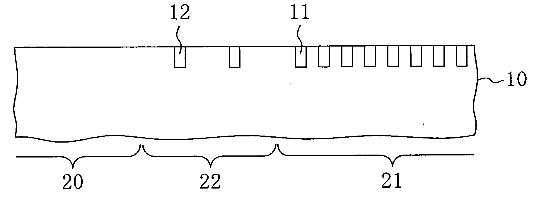
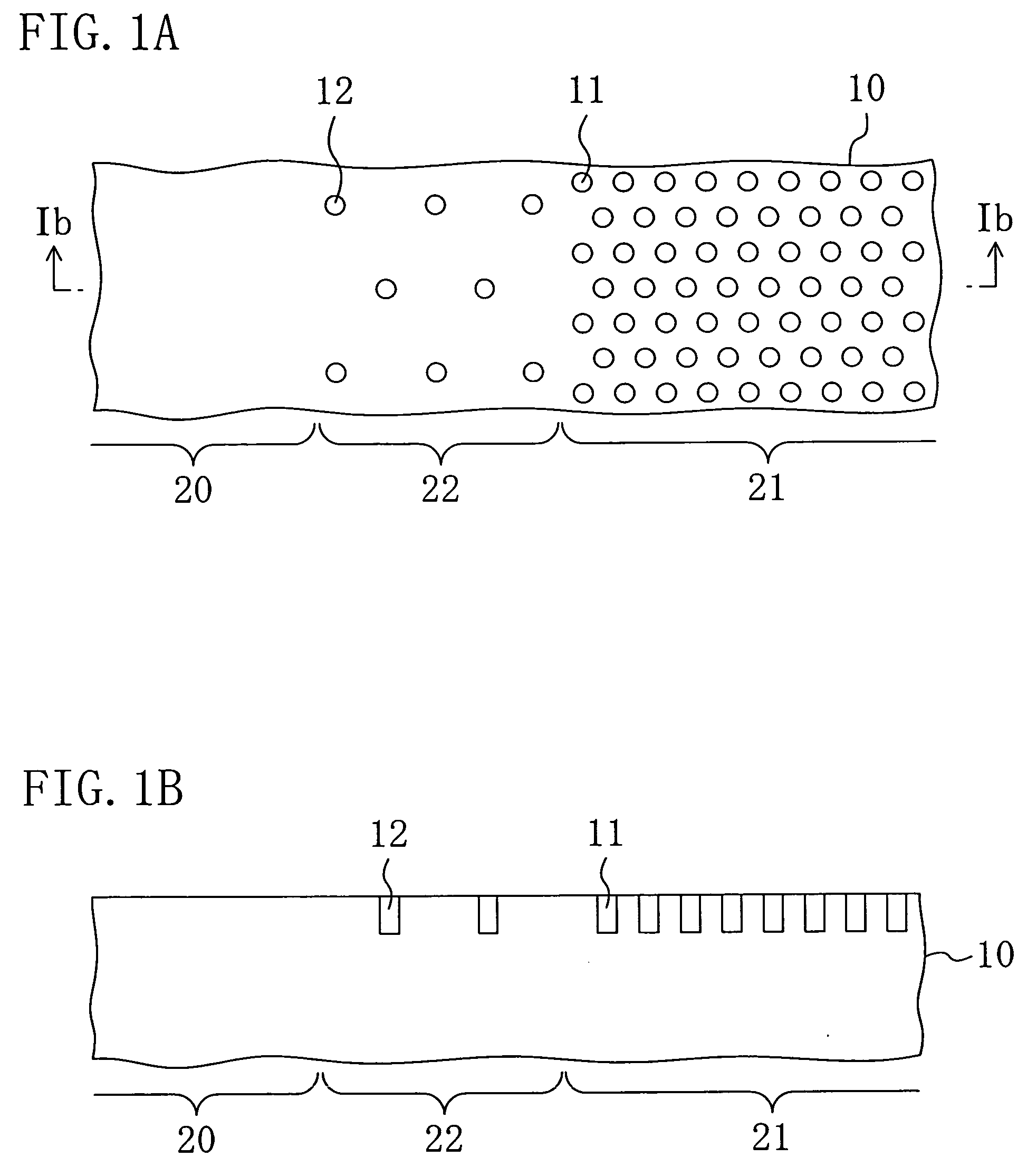
[0044]A first embodiment of the present invention will be described with reference to the accompanying drawings. FIGS. 1A and 1B illustrate a substrate for forming a semiconductor device according to the first embodiment. FIG. 1A shows a plan structure thereof, and FIG. 1B shows a cross-sectional structure thereof taken along the line Ib-Ib in FIG. 1A.

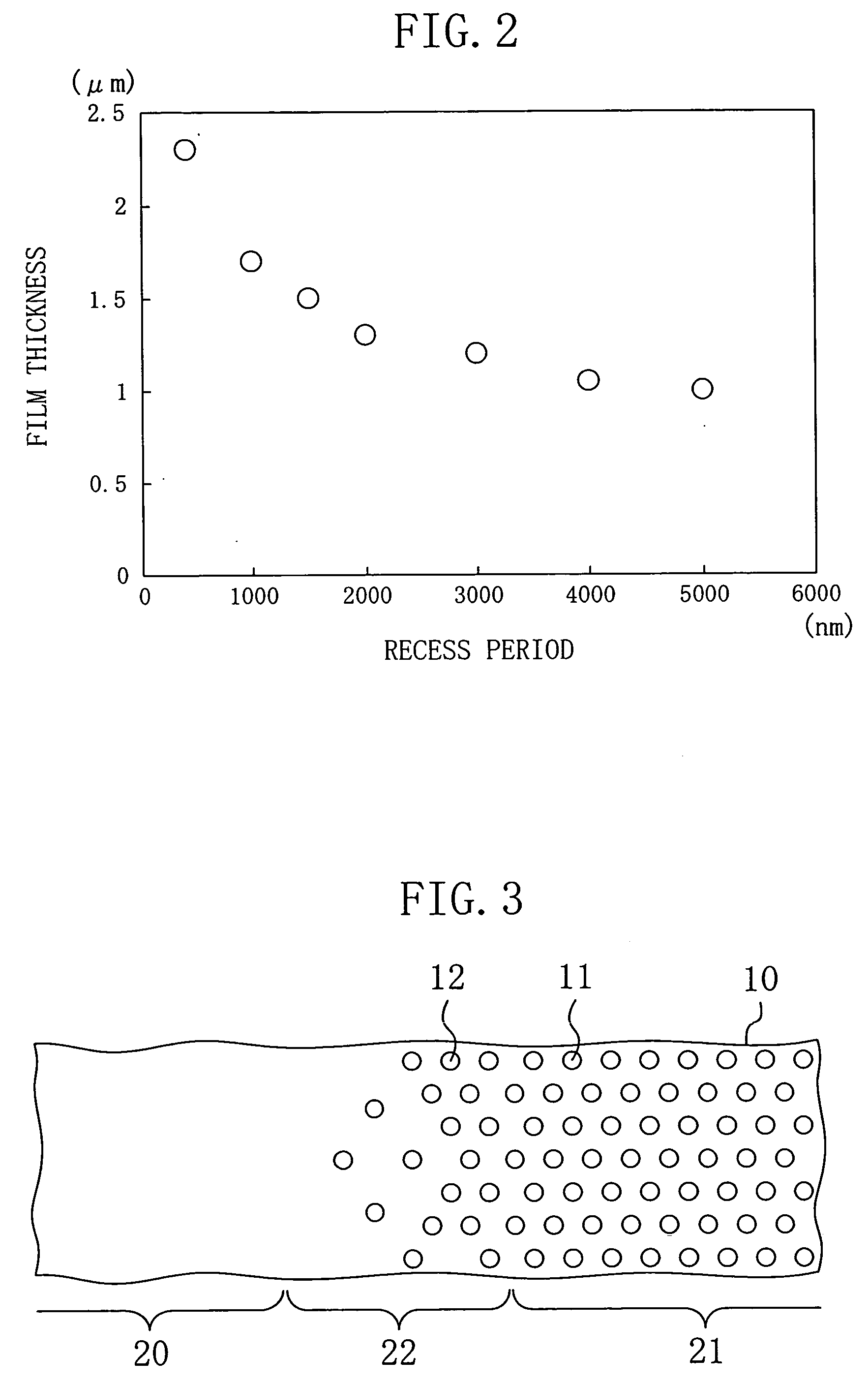
[0045]The main surface of a substrate 10 is provided with: a flat region 20; a first indentation region 21 formed with first recesses 11; and a second indentation region 22 located between the flat region 20 and the first indentation region 21 and formed with second recesses 12 having a lower density than the first recesses 11.

[0046]In the case of forming a photonic crystal, in the first indentation region 21, the first recesses 11 are formed in a lattice pattern having a period almost the same in length as the wavelength of light emitted from an LED. For example, for a general GaN-based LED with a wavelength of 450 nm, it is sufficien...

second embodiment

[0064]A second embodiment of the present invention will be described below with reference to the accompanying drawings. FIG. 8 shows a cross-sectional structure of a semiconductor device according to the second embodiment. Referring to FIG. 8, the semiconductor device of the second embodiment is a light emitting diode (LED), and includes a substrate 30 made of sapphire and a semiconductor layer 50 formed on the substrate 30.

[0065]The substrate 30 is provided with: a flat region 40; a first indentation region 41 formed with first recesses 31; and a second indentation region 42 located between the flat region 40 and the first indentation region 41 and formed with second recesses 32 having a lower density than the first recesses 31. The first recesses 31 each have a diameter of 200 nm and a depth of 150 nm, and are arranged in a triangular lattice pattern having a period of 400 nm. The second recesses 32 each have a diameter of 200 nm and a depth of 150 nm, and are arranged in a triang...

third embodiment

[0070]A third embodiment of the present invention will be described below with reference to the accompanying drawings. FIG. 9 shows a cross-sectional structure of a semiconductor device according to the third embodiment. Referring to FIG. 9, the semiconductor device of the third embodiment is an LED having a photonic crystal formed on an emitting surface. Above a holding substrate 87, a semiconductor layer made by sequentially staking a p-type GaN layer 83, an InGaN active layer 82, and an n-type GaN layer 81 is held with a p-side electrode 84 interposed therebetween. On the n-type GaN layer 81, an n-side electrode 85 is formed, and photonic crystals each having a diameter of 200 nm and a height of 150 nm are arranged in a triangular lattice pattern having a period of 400 nm.

[0071]FIGS. 10A to 10D show a method for fabricating an LED with a photonic crystal according to the third embodiment in the order of its fabrication process steps. Referring to FIG. 10A, first, a first indentat...


PUM


Abstract

A semiconductor device includes a substrate and a semiconductor layer formed on the substrate. The substrate has: a flat region provided in a main surface thereof; a first indentation region provided in a portion of the main surface different from the flat region and formed with first recesses; and a second indentation region provided between the first indentation region and the flat region, formed with second recesses, and having a lower probability of occurrence of growth nuclei than the first indentation region and a higher probability than the flat region in the case where a crystal of a semiconductor is grown on the main surface.

Description

CROSS-REFERENCE TO RELATED APPLICATIONS[0001]This application claims priority under 35 U.S.C. § 119 on Patent Application No. 2006-011969 filed in Japan on Jan. 20, 2006, the entire contents of which are hereby incorporated by reference.BACKGROUND OF THE INVENTION[0002](a) Fields of the Invention[0003]The present invention relates to semiconductor devices and their fabrication methods.[0004](b) Description of Related Art[0005]In growing a semiconductor layer on a substrate, crystal growth of the semiconductor may be conducted on an indented surface of the substrate. For example, a crystal of a semiconductor layer is grown on a substrate with fine indentations, whereby the crystallinity of the formed semiconductor layer is improved. This provides a semiconductor device with excellent characteristics (see, for example, Japanese Unexamined Patent Publication No. 2002-289540).[0006]For a semiconductor light emitting diode (LED), a photonic crystal having two-dimensionally periodic inden...

Claims


Application Information

Patent Timeline
IPC IPC(8): H01L29/06H01L33/16H01L33/22H01L33/32
CPCG02B2006/1213H01L33/007H01L33/005
Inventor TAKASE, YUJI
Owner PANASONIC CORP
Why Eureka
Try Eureka