Semiconductor device and fabrication method thereof

a semiconductor and semiconductor technology, applied in the field of microelectromechanical (mems) devices, can solve the problems of large die size, and inability to efficiently facilitate the formation of thick capacitor gaps

Active Publication Date: 2007-07-26
TEXAS INSTR INC
View PDF9 Cites 27 Cited by
  • Summary
  • Abstract
  • Description
  • Claims
  • Application Information

AI Technical Summary

Benefits of technology

[0008] According to another aspect of the invention, an acceleration sensor is fabricated over active circuitry, for example, after the formation of transistor devices and after formation of a pre-metal dielectric (PMD) layer with contacts formed therein down to the active circuitry. The formation of the acceleration sensor comprises forming conductive electrode layers with low temperature processing techniques such as sputtering or physical vapor deposition at temperatures less than 600 C. In one example of the invention, an insulative protective layer is formed over the bottom electrode layer, and other insulative protective layers are formed on the top and bottom of the upper electrode layer. In such example, a sacrificial gap layer is formed between the insulative protective layers and comprises aluminum that exhibits a fast deposition rate, thereby efficiently facilitating formation of a thick capacitor gap of, for example, 1-5 microns. Subsequently, the sacrificial gap layer is removed via, for example, a wet etch that is selective with respective to the insulative protective layers to thereby define the gap.

Problems solved by technology

Prior art MEMS acceleration sensor systems were not space efficient.
This lateral juxtaposition of the MEMS sensor and the active circuitry disadvantageously increases the die size, thereby causing such integrated circuit chips to be rather expensive.

Method used


Image

  • Semiconductor device and fabrication method thereof
  • Semiconductor device and fabrication method thereof
  • Semiconductor device and fabrication method thereof

Examples


Embodiment Construction

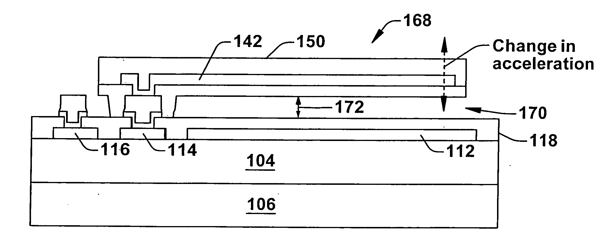
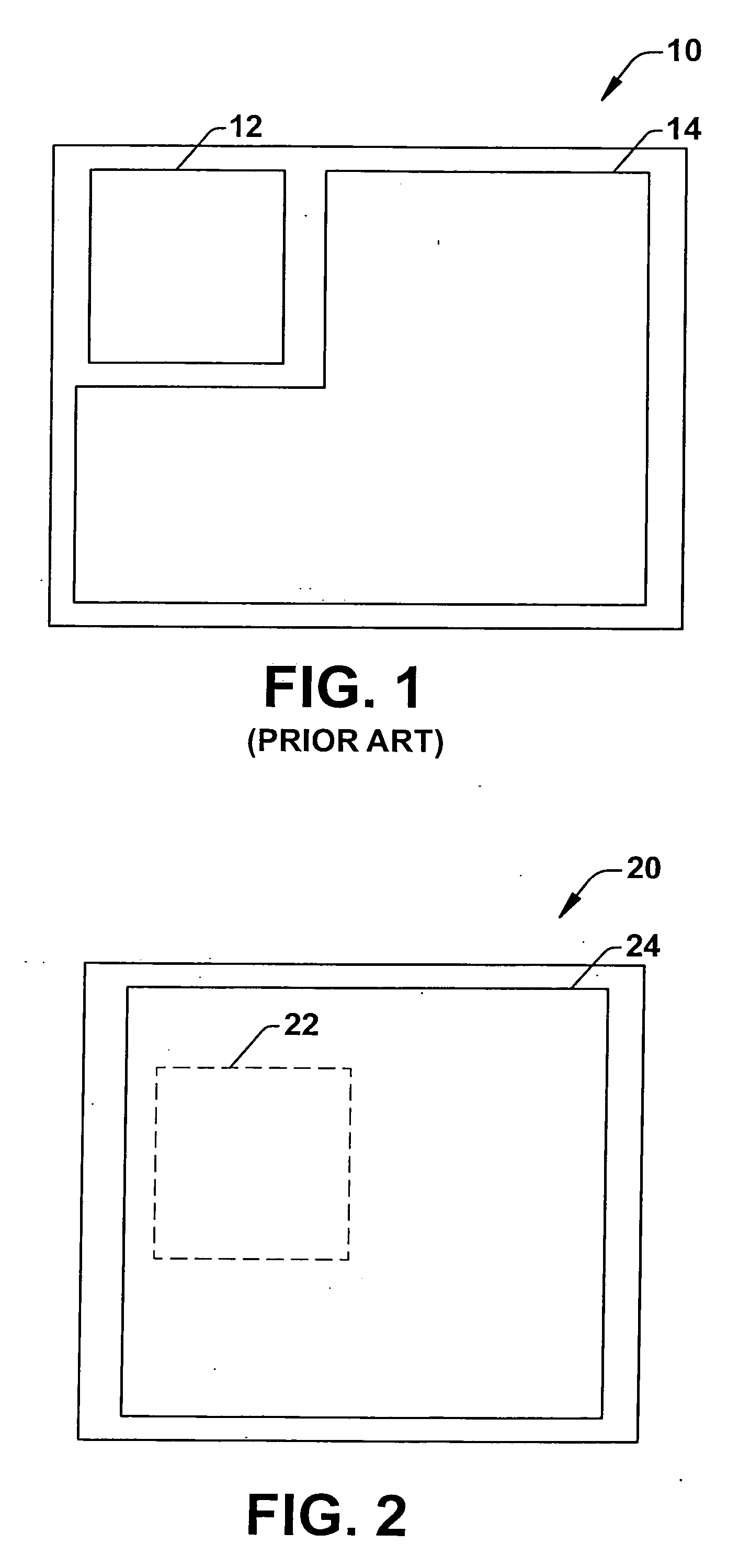
[0015] The present invention will now be described with reference to the attached drawings, wherein like reference numerals are used to refer to like elements throughout. The invention is directed to a method of forming a MEMS structure such as an acceleration sensor over active circuitry. For example, active circuitry according to the present invention may include a metal circuit wiring layer or multiple wiring layers (e.g., aluminum, titanium tungsten, titanium nitride, tungsten, platinum and / or other conductive materials). The method employs low temperature processing (e.g., less than about 600 degrees-C.) of the MEMS structure, thereby facilitating fabrication of the MEMS structure without substantially affecting electrical characteristics of the active circuitry therebelow. A simplified, plan view of one example of such an integrated circuit device is illustrated in FIG. 2, wherein a device 20 has a MEMS structure 22 (shown in phantom) formed over active circuitry 24 according ...


PUM


Abstract

A method of forming a MEMS structure over active circuitry in a semiconductor body includes forming active circuitry in a semiconductor body, and forming the MEMS structure over the active circuitry, wherein at least a portion of the MEMS structure spatially overlaps the active circuitry.

Description

FIELD OF INVENTION [0001] The present invention relates generally to micro-electromechanical (MEMS) devices and to a method of fabrication thereof. More particularly, the invention relates to a method of forming a MEMS device such as an acceleration sensor or inertial sensor over active circuitry of an integrated circuit device, thereby minimizing die size. BACKGROUND OF THE INVENTION [0002] Current trends in the semiconductor and electronics industry require memory devices to be made smaller, faster and require less power consumption. In addition to active circuitry on such integrated circuit devices, micro-electromechanical (MEMS) devices are sometimes employed in various applications. One exemplary application involves aircraft or vehicle applications, where a MEMS device is employed to detect a change in acceleration. In early systems, the active circuitry was manufactured separately from the MEMS device, however, in recent years attempts have been made to integrate the MEMS dev...

Claims


Application Information

Patent Timeline
Patent Type & Authority Applications(United States)
IPC IPC(8): H01L21/8232H01L21/335H01L21/00
CPCB81B2201/025B81C1/00246H01L27/0688G01P15/0802G01P15/125B81C2203/0735G01P2015/0828
Inventor TOMOMATSU, HIROYUKIWATANABE, KAZUHIKOTADA, TETSUYATANI, TOSHIYUKI
Owner TEXAS INSTR INC
Why Eureka
Try Eureka