Nanotube sensor devices for DNA detection

a dna detection and nanotube technology, applied in the field of sensors, can solve the problems of expensive, slow, complex, unlikely to be useful for routine medical testing, and the chemical reaction by which the dna is labeled is expensive and time-consuming

Inactive Publication Date: 2007-08-02
NANOMIX
View PDF52 Cites 66 Cited by
  • Summary
  • Abstract
  • Description
  • Claims
  • Application Information

AI Technical Summary

Benefits of technology

[0029] A sensor device may be used by exposing the nanotube network to a solution containing sample ssDNA. The network should be exposed to the solution for a period of time long enough for hybridization to occur. This period of time depends on the concentration of the sample DNA, the quantity of the solution, the temperature of the room, the pH of the solution, and other variables. Those skilled in the art are familiar with the effect of these variables on DNA hybridization and are capable of choosing an appropriate period of time, solution composition, temperature and other conditions of hybridization without undue experimentation.

Problems solved by technology

These techniques have shortcomings that make them expensive, slow, and complex, so that they are unlikely to be useful for routine medical testing.
Although the use of optical detection makes this approach convenient, the chemical reaction by which the DNA Is labeled is expensive and time-consuming.
A second problem results from the low sensitivity of traditional detection methods.
Although some of these methods are sensitive to low concentrations of DNA, they require large absolute numbers of DNA molecules.
Like labeling, PCR is a complex chemical reaction, which makes tests expensive and slow.

Method used


Image

  • Nanotube sensor devices for DNA detection
  • Nanotube sensor devices for DNA detection
  • Nanotube sensor devices for DNA detection

Examples


example a

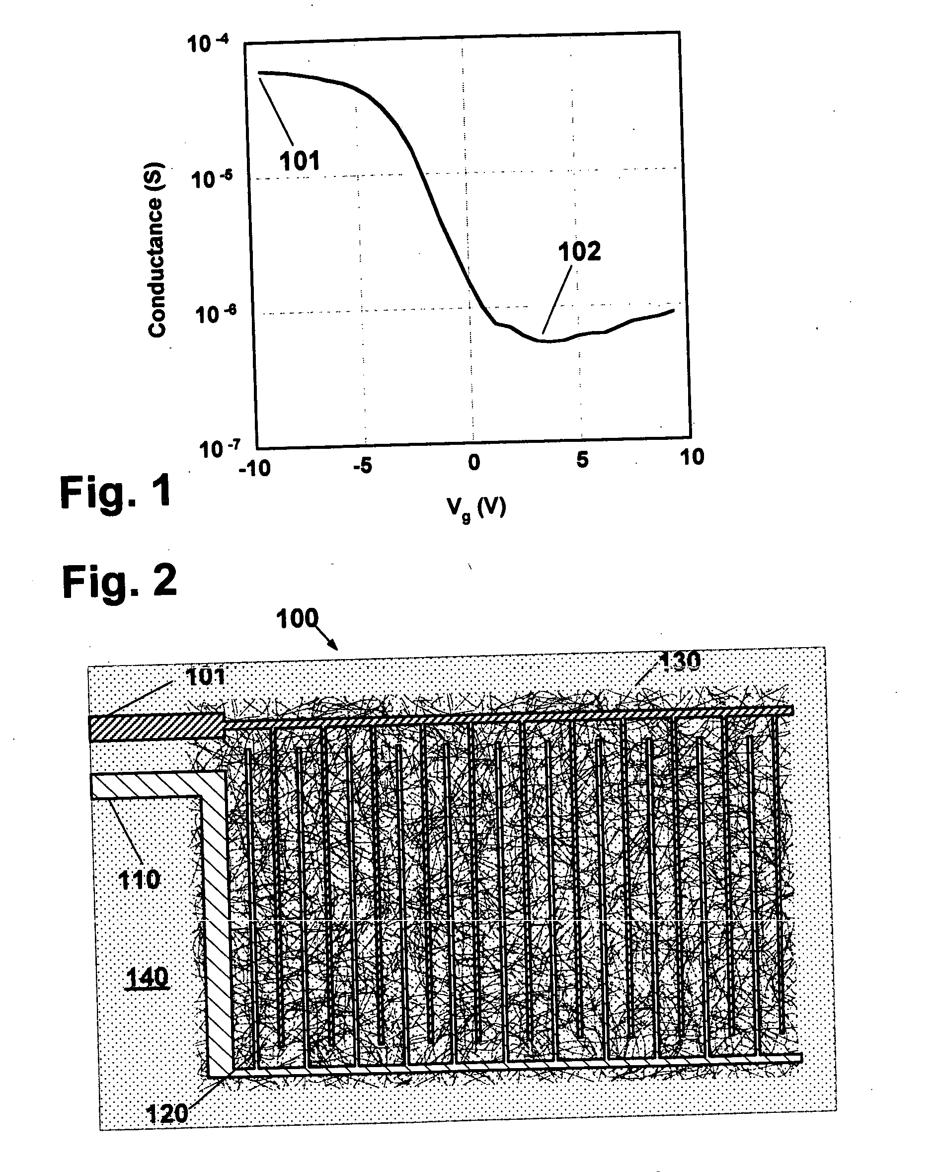
[0087] A degenerately doped silicon wafer with a silicon oxide film was coated with carbon nanotubes in a random network, as described in the earlier-referenced U.S. patent application Ser. No. 10 / 177,929 and generally in accordance with the description hereinabove. Titanium contacts 30 nm thick covered with gold contacts 120 nm thick were deposited and patterned by photolithography and lift-off to form opposing contacts. The contacts each comprised a plurality of interdigitated portions disposed over a generally rectangular region. A network of randomly oriented nanotubes was disposed over the silicon substrate. Nanotubes in the network were in electrical contact with interdigitated portions of the contacts. After the deposition of the contacts, nanotubes outside of the generally rectangular area were removed by oxygen plasma etching, leaving nanotube network remaining. The use of interdigitated sets of metal electrodes with nanotube network interposed generally between the interdi...

example b

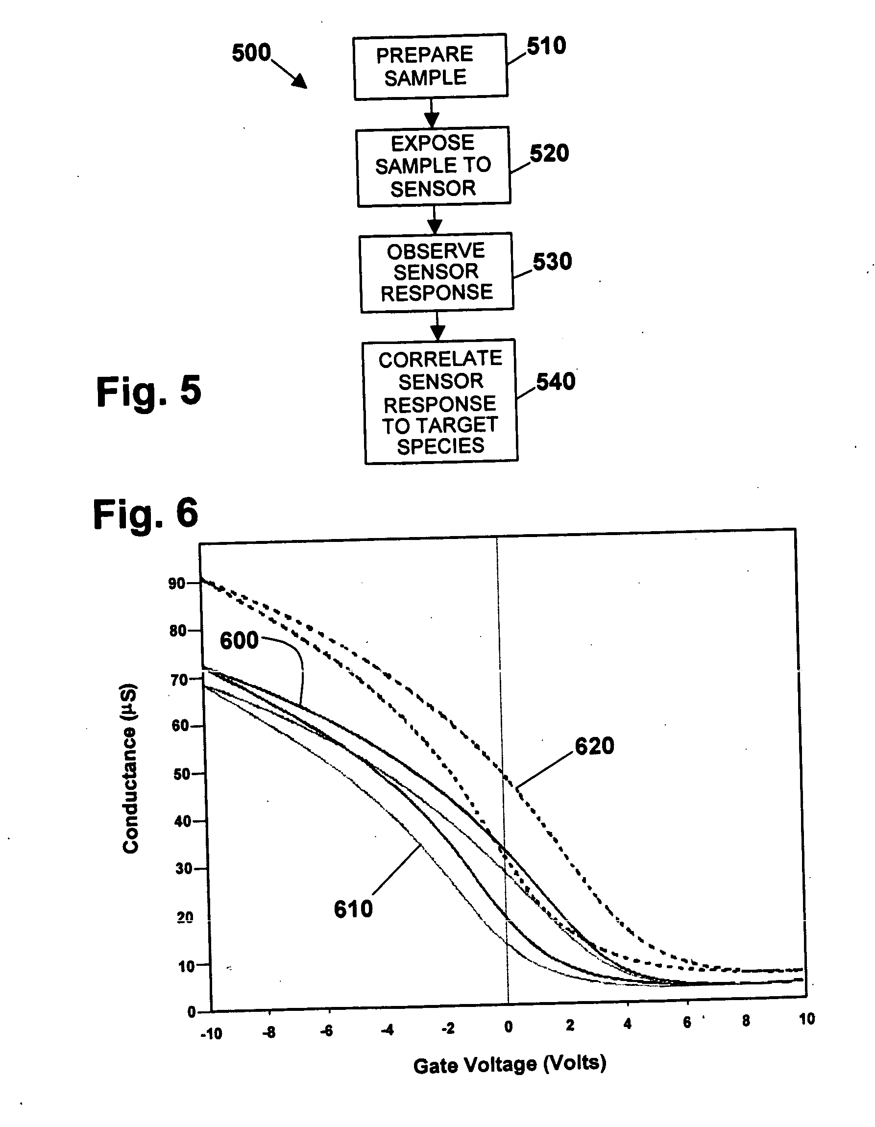
Noncovalent Chemical Functionalization of Carbon Nanotube Devices for Single Base Mismatch DNA detection.

[0093] B-1. Summary:

[0094] In one exemplary embodiment having aspects of the invention, a nanotube sensor device comprises a carbon nanotube network field effect transistor (“NTFET” or “NTNFET”) device functionalized with single-stranded DNA (ssDNA). In certain embodiments, single-stranded DNA (ssDNA) may be immobilized on NTFET devices through polymer and polyaromatic molecules non-covalently attached to carbon nanotubes. The significant differences in the electronic response of functionalized NTFETs to complementary single-stranded DNA (cDNA) and single base mismatch single-stranded DNA (sbmDNA) may be measured. This exemplary sensor includes the following structure, elements and functions:

[0095] a) One or more carbon nanotube FET device comprising a single nanotube and / or a networks of nanotubes disposed to form a conducting channel between at least a source and a drain ele...

example c

[0122] DNA assays using nanoelectronic devices.

[0123] A number of different exemplary DNA (or other polynucleotide) assay embodiments having aspects of the invention are shown in FIGS. 8-12. The structure and methods shown are exemplary, and other alternative embodiments may use structures and methods described elsewhere in this application. Where the different embodiments include substantially similar elements, the same reference numbers are used to designate such elements in the description of each embodiment.

C-1 Structure:

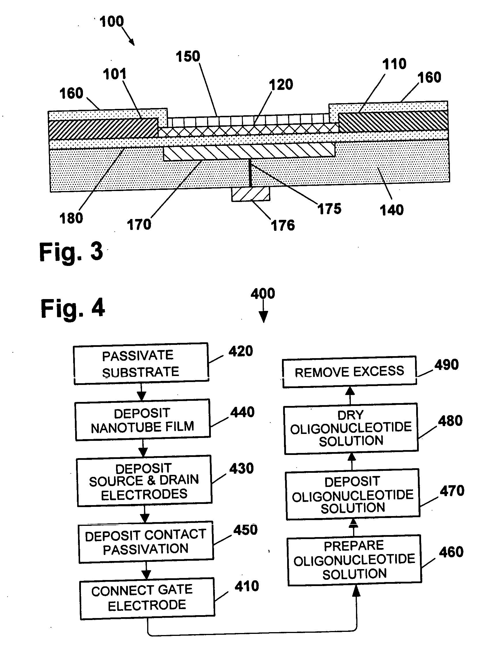
[0124] As shown in FIGS. 8-9, and also in FIGS. 10-12, the sensor 10 comprises a platform having at least one nanostructure, such as nanotube 12 disposed adjacent substrate 14 and in electrical communication between at least a source electrode 16 and a drain electrode 18.

[0125] Optionally, the device may include at least one additional electrode, such as gate electrode 20 disposed adjacent nanotube 12. The gate electrode 20 is shown embedded in substrate 14...


PUM

PropertyMeasurementUnit
gate voltageaaaaaaaaaa
gate voltagesaaaaaaaaaa

Abstract

A nanotube device is configured as an electronic sensor for a target DNA sequence. A film of nanotubes is deposited over electrodes on a substrate. A solution of single-strand DNA is prepared so as to be complementary to a target DNA sequence. The DNA solution is deposited over the electrodes, dried, and removed from the substrate except in a region between the electrodes. The resulting structure includes strands of the desired DNA sequence in direct contact with nanotubes between opposing electrodes, to form a sensor that is electrically responsive to the presence of target DNA strands. Alternative assay embodiments are described which employ linker groups to attach ssDNA probes to the nanotube sensor device.

Description

CROSS-REFERENCE TO RELATED APPLICATION [0001] This application claims priority pursuant to 35 U.S.C. §119(e) to U.S. Provisional Application No. 60 / 604,293, filed Aug. 24, 2004, and to U.S. Provisional Application No. 60 / 629,604, filed Nov. 19, 2004, each of which applications is specifically incorporated herein, in its entirety, by reference. [0002] This application also claims priority as a continuation-in-part of U.S. patent application Ser. No. 10 / 345,783 filed Jan. 16, 2003, entitled “Electronic Sensing of Biological and Chemical Agents Using Functionalized Nanostructures” (now published as 2003-0134433), which claims priority to U.S. Provisional Patent Application No. 60 / 349,670 filed Jan. 16, 2002; each of which applications is specifically incorporated herein, in its entirety, by reference. [0003] This application also claims priority as a continuation-in-part of U.S. patent application Ser. No. 10 / 704,066 filed Nov. 7, 2003 entitled “Nanotube-Based Electronic Detection Of B...

Claims


Application Information

Patent Timeline
Patent Type & Authority Applications(United States)
IPC IPC(8): C12Q1/68C12M3/00
CPCC12Q1/6825G01N27/4146G01N27/4145C12Q2565/631C12Q2565/107
Inventor JOINER, CHARLES S. JR.GABRIEL, JEAN-CHRISTOPHE P.GRUNER, GEORGESTAR, ALEXANDER
Owner NANOMIX
Why Eureka
Try Eureka