Sputtering system providing large area sputtering and plasma-assisted reactive gas dissociation

a technology of sputtering system and reactive gas, which is applied in the direction of vacuum evaporation coating, electrolysis components, coatings, etc., can solve the problems of difficult to produce transparent electronic circuits with silicon-based materials, insufficient performance of silicon-based electronic devices, and inconvenient use of silicon-based materials. , to achieve the effect of improving the quality of semiconductor elements formed with thin films

Inactive Publication Date: 2007-08-09
IND TECH RES INST
View PDF12 Cites 34 Cited by
  • Summary
  • Abstract
  • Description
  • Claims
  • Application Information

AI Technical Summary

Benefits of technology

[0008] One objective of the present invention is to provide a sputtering system providing large area sputtering and plasma-assisted reactive gas dissociation, which has a plurality of plasma sources to dissociate different reactive gases so as to dope the dissociated reactive gases in the thin film during the deposition of the thin film, and the composition of the thin film can be controlled and the property of the thin film is improved.
[0009] It is another objective of the present invention to provide a sputtering system providing large area sputtering and plasma-assisted reactive gas dissociation, in which different plasma sources are used to dissociate different reactive gases in different time sequence such that a composite film can be formed on a substrate.
[0013] The remote plasma sources can be positioned outside or within the reaction chamber in the present invention. The different reactive gases can be effectively dissociated by the different plasma sources of the present invention such that the dissociated reactive gases can be doped into a thin film during the thin film deposition to control the composition of the thin film. The quality of semiconductor elements formed with the thin film can be improved.

Problems solved by technology

It is a challenge to produce high-performance devices with silicon-based materials by low-temperature manufacturing processes.
However, the performance of the devices is constricted due to low electrons mobility of the channel material.
In practice, the performances of these silicon-based electronic devices haven't been sufficient to be as the transistors applicable in the calculators and current-driven organic light-emitting diode display (OLED).
It is not easy to produce transparent electronic circuit with the silicon-based material.
Because some targets are expensive, when adopting magnetic field to bound electrons on the surface of the target, it will cause un-evenly sputtering on the target.

Method used


Image

  • Sputtering system providing large area sputtering and plasma-assisted reactive gas dissociation
  • Sputtering system providing large area sputtering and plasma-assisted reactive gas dissociation
  • Sputtering system providing large area sputtering and plasma-assisted reactive gas dissociation

Examples


Embodiment Construction

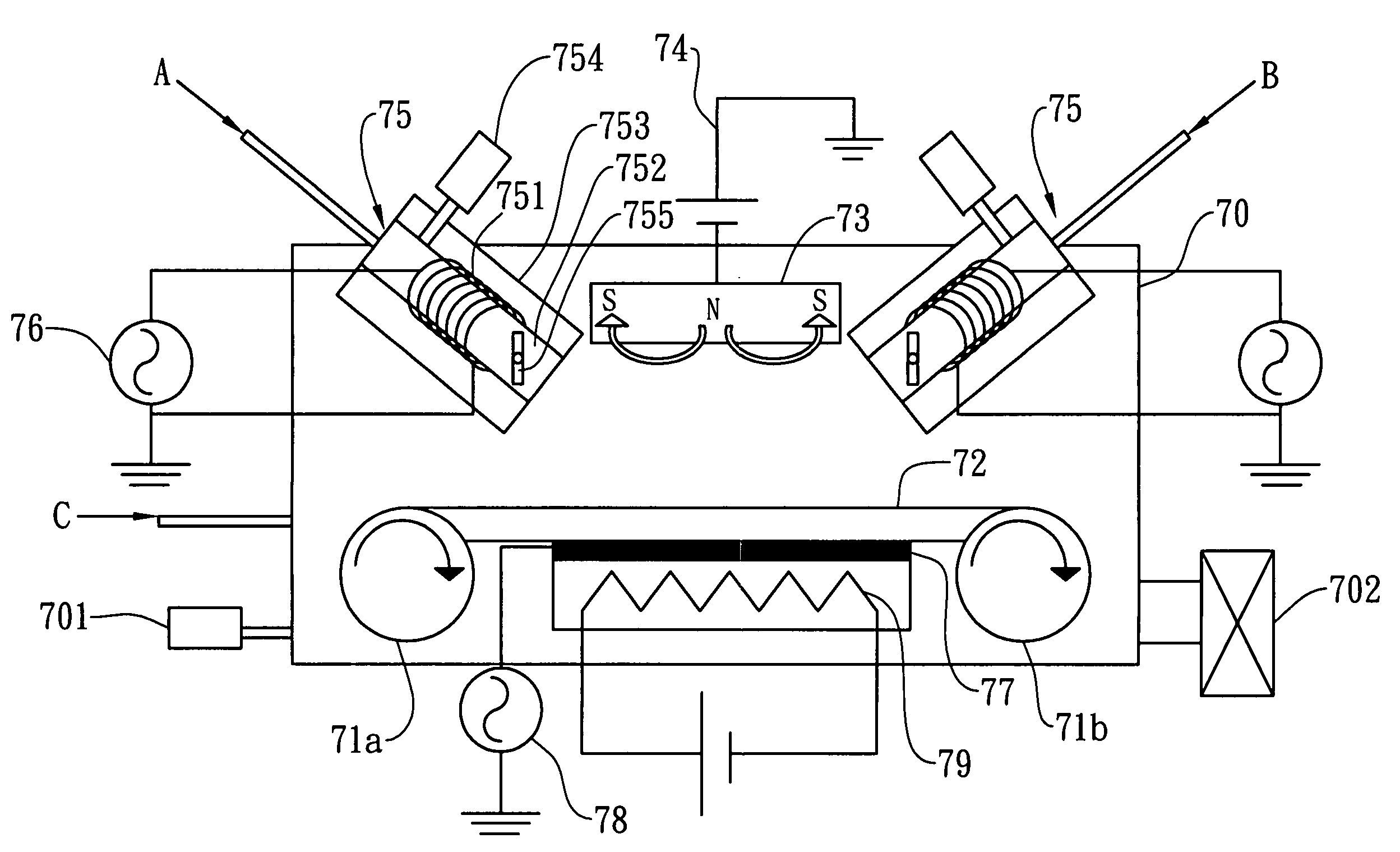
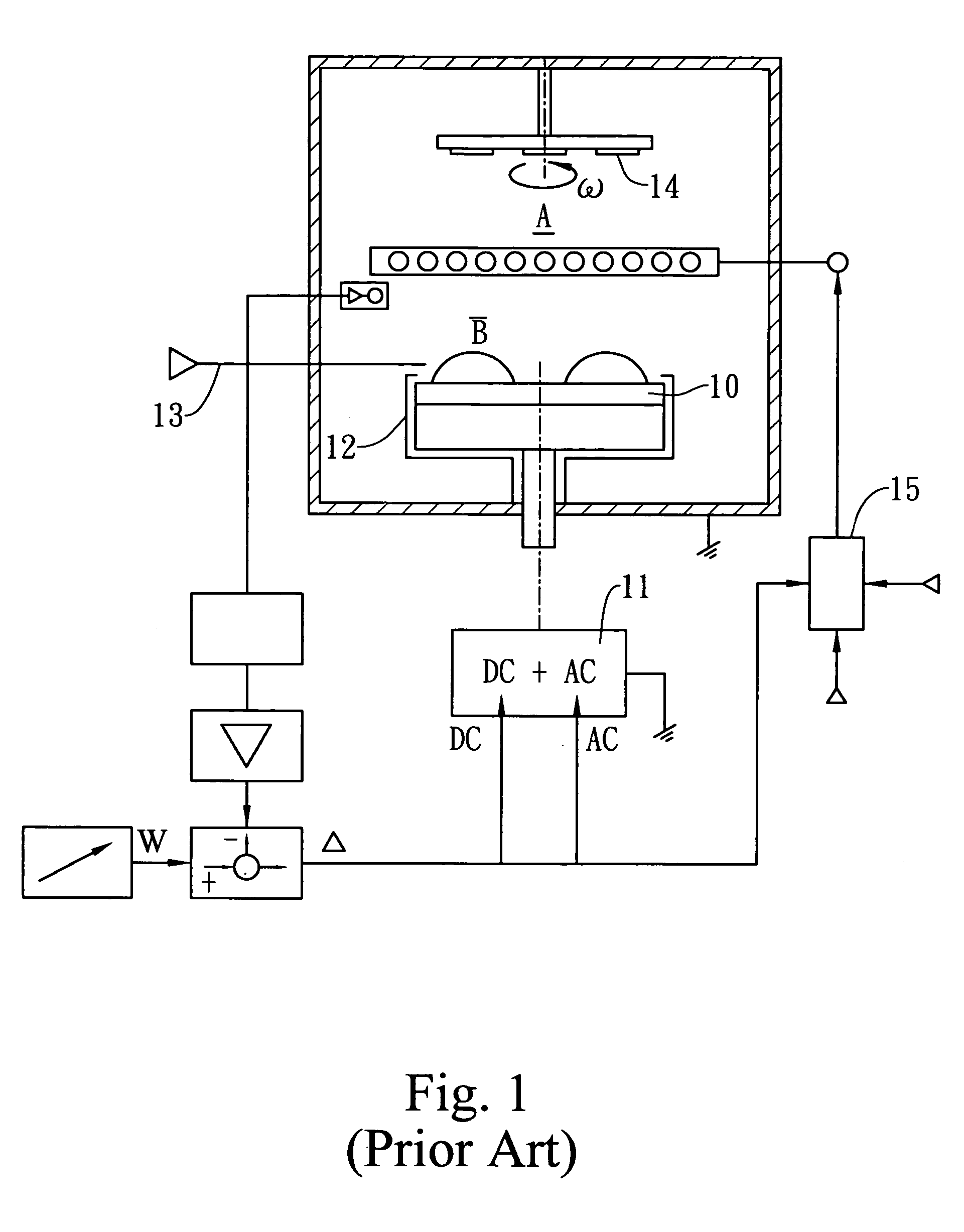
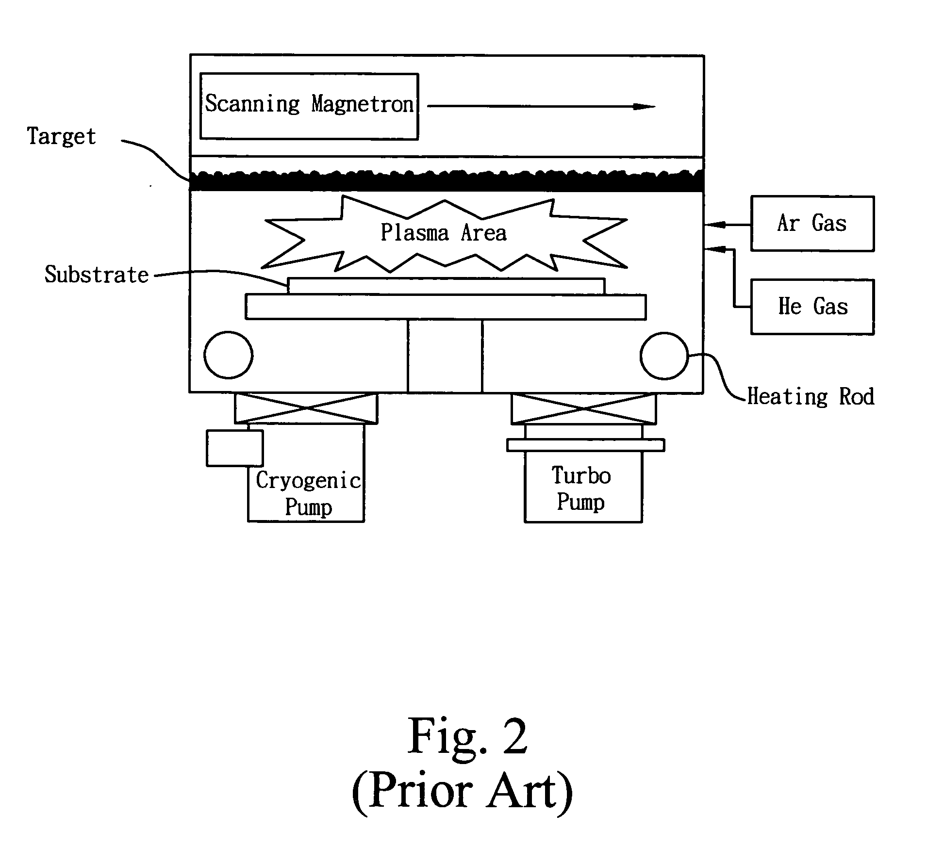
[0028] The present invention provides a sputtering system providing large area sputtering and plasma-assisted reactive gas dissociation, which comprises a plurality of plasma sources. By the plasma sources the reactive gases are dissociated to become atoms and ions, and being doped into a deposition film during a sputtering process for forming the deposition film. By controlling the plasma powers, the pressures of the plasma sources and flow rates of the reactive gases a specific component content of the deposition film can be controlled, and thus improving the quality of the film. The plasma source used to dissociate the reactive gases in the present invention can be inductively coupled plasma source or capacitively coupled plasma source. Further, when the area of the substrate is enlarged, the present sputtering system can use two plasma sources or more positioned in a line to dissociate the reactive gases to become atoms and ions, and hence the atoms and ions can be evenly dispos...


PUM

PropertyMeasurementUnit
areaaaaaaaaaaa
bias voltageaaaaaaaaaa
pressureaaaaaaaaaa

Abstract

This invention provides a sputtering system providing large area sputtering and plasma-assisted reactive gas dissociation. A plurality of plasma sources is provided in a reaction chamber to dissociate at least one reactive gas. The dissociated reactive gas is doped in a film during the deposition of the film so as to control the composition of the film. The property of the film is thus improved. A composite film can be formed on the substrate by the present sputtering system. The present sputtering system is suitable for film deposition on a large-area hard substrate and flexible substrate.

Description

BACKGROUND OF THE INVENTION [0001] 1. Field of the invention [0002] The present invention relates to a sputtering system provided with a plurality of reactive gas plasma sources; more particularly to a sputtering system providing large area sputtering and plasma-assisted reactive gas dissociation. [0003] 2. Description of the Related Art [0004] The silicon-based electronic devices need to take a trade-off between manufacturing temperatures and characteristics of the devices. It is a challenge to produce high-performance devices with silicon-based materials by low-temperature manufacturing processes. The low-temperature manufacturing process of thin film transistors can improve the development of the flexible electronic devices. These devices, such as large size high resolution display, wearable calculator and film-like display etc, have characteristics of flexible, light-weight, impact-resistant and low cost. As so far, the flexible electronic devices mainly adopt hydrogenated amorp...

Claims


Application Information

Patent Timeline
Patent Type & Authority Applications(United States)
IPC IPC(8): C23C14/00
CPCC23C14/0047C23C14/354C23C14/358H01J37/3438H01J37/32357H01J37/3408C23C14/562
Inventor WEI, HUNG-WENTING, HUNG-CHECHEN, HSUEH-YING
Owner IND TECH RES INST
Why Eureka
Try Eureka