Semiconductor device and method of forming the same

a technology of semiconductor devices and semiconductors, applied in the direction of semiconductor devices, basic electric elements, electrical appliances, etc., can solve the problems of unfavorable jfet resistance increase, high cost of sic wafers in comparison with sic wafers, and high cost of sic wafers

Inactive Publication Date: 2007-08-16
FUJI ELECTRIC HLDG CO LTD
View PDF9 Cites 62 Cited by
  • Summary
  • Abstract
  • Description
  • Claims
  • Application Information

AI Technical Summary

Problems solved by technology

Mass producing SiC devices, however, can be problematic in that an SiC wafer is very expensive in comparison with an Si wafer.
Such increase in the JFET resistance is unfavorable because it increases the loss in the on-state.
However, an electric field with high strength applied to the insulator for a long time deteriorates the insulator gradually over time until it eventually breaks down.
Therefore, should the source and the drain be short-circuited, only the device is burnt out, or only a few other power devices operating in cooperation with the device or only passive elements are burnt out.
Therefore, when a high voltage on the drain side is applied to the gate by a short circuit between the gate and the drain, the control circuit on the gate side become damaged.
Then, the destructive high voltage is transmitted from the control circuit to the neighboring low voltage circuits from one to another to possibly causing fatal damages of the entire system using the power device.
This, however, is not only economically undesirable but also decreases performance, such as by increasing the switching loss, reducing the switching speed, and distorting the control signal waveform due to charge and discharge of the Zener diode carried out at each switching.
Thus, it is not desirable to incorporate such a design where the breakdown voltage of the device is determined by the breakdown voltage between the gate and the drain.
However, a vertical trench MISFET using SiC, otherwise having the same structure as the Si device as shown in FIG. 16 causes the following problem.
This, like in the case in the DMOSFET structure, imposes limitation on reducing the cell pitch.
Therefore, as was explained above, in an SiC device using an expensive SiC wafer, despite the importance of cell pitch reduction, the main effect of reducing the cell pitch, which is obtained by providing the trench MOSFET type structure, is lost.
Furthermore, the structure disclosed in JP-A-10-308512 has a drawback in that it prevents realization of a high breakdown voltage expected from the high value of the insulation breakdown electric field strength of SiC.

Method used


Image

  • Semiconductor device and method of forming the same
  • Semiconductor device and method of forming the same
  • Semiconductor device and method of forming the same

Examples


first embodiment

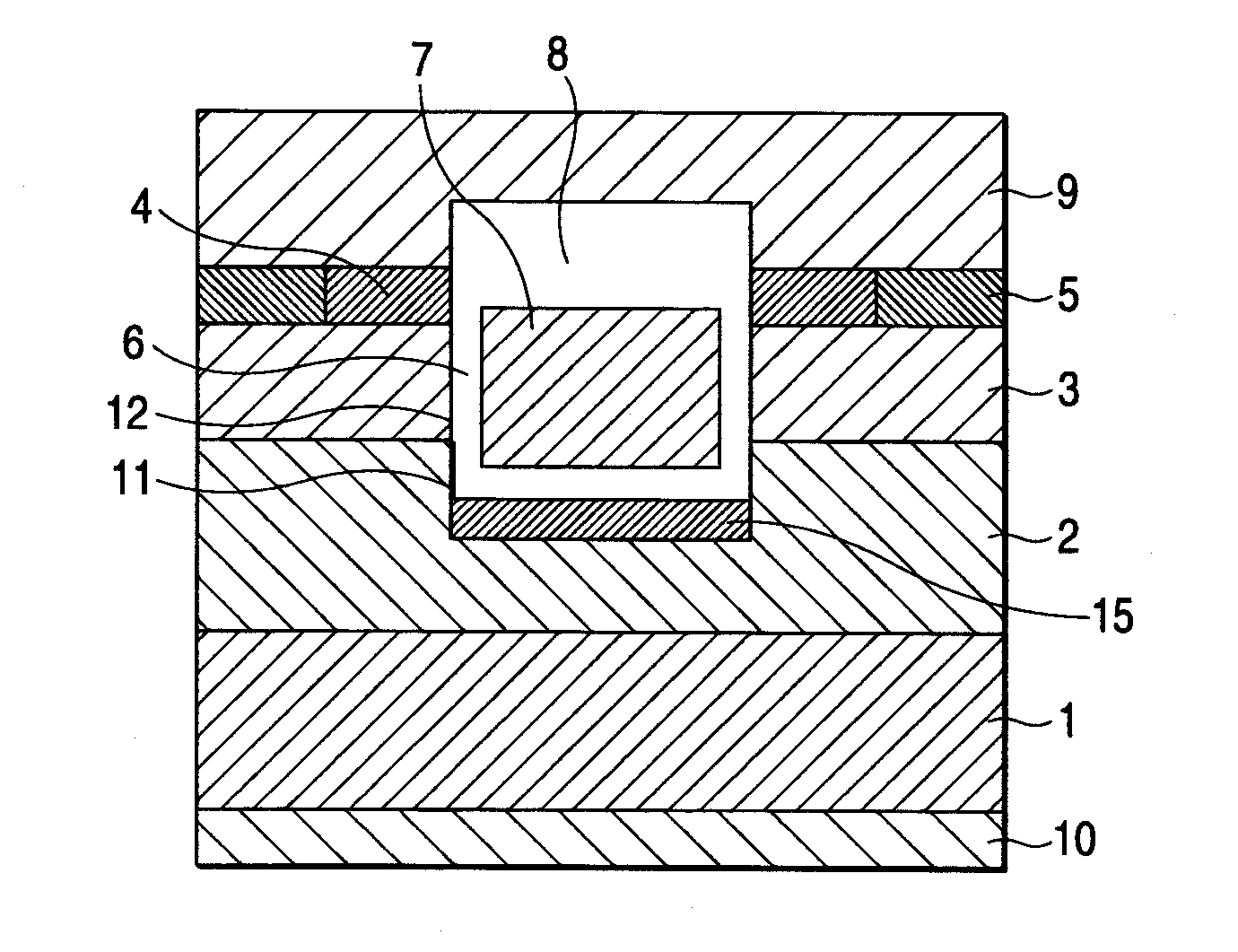
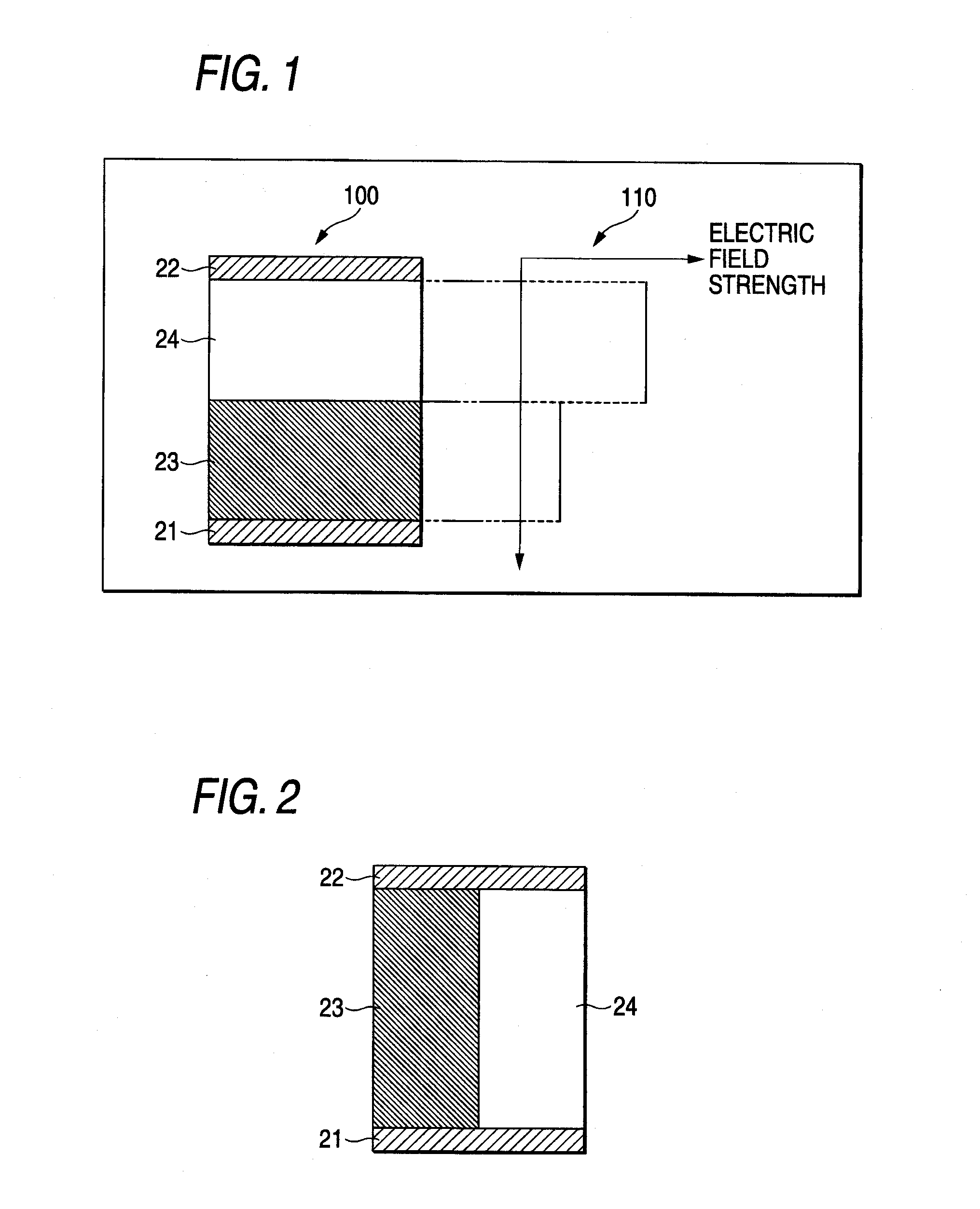
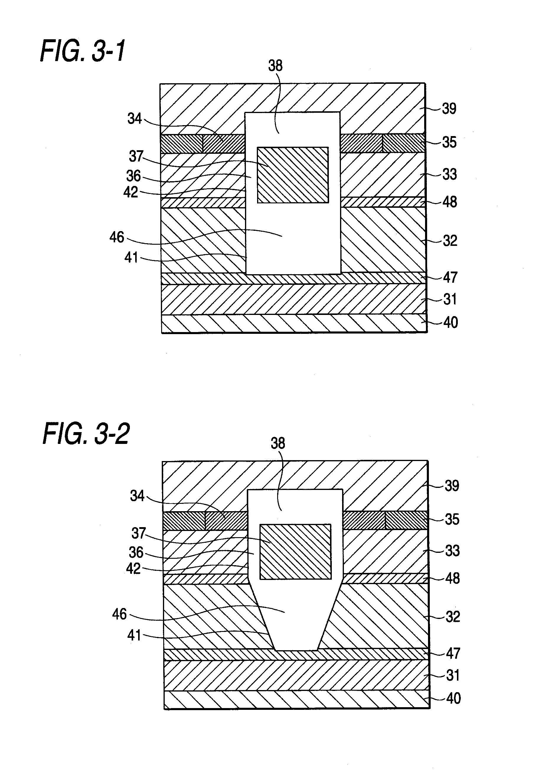
[0080] Normally, in a vertical MISFET, a highly doped layer known as a field stopping layer is provided on the drain side. After the drift layer is completely made depleted, the electric field strength abruptly reduces in the field stopping layer to almost zero. The section deeper than this, like becomes part of the drain electrode. Therefore, as shown in, for example, FIG. 3-1, in a semiconductor device according to the present invention, the depth of the trench 41 is configured so that the electric field strength therein becomes approximately zero, at least the insulation breakdown voltage on the semiconductor side. Moreover, in the section of the trench in the vicinity of a MIS channel 42, i.e., a section deeper than a gate electrode 37, an insulator 46 is kept buried. Such a structure enables realization of the electrical properties shown in FIG. 2.

[0081] Moreover, when the normal insulation breakdown electric field strength of the insulator 46 buried in a deep section in the tr...

second embodiment

[0197] Referring to FIG. 14, which shows an arrangement of a principal part of a trench MOSFET according to the present invention, as shown by the cross-sectional view 1400 the trench 41 is formed to penetrate through the field stopping layer 47 and reach a deeper section in the substrate 31. Moreover, as shown in the side cross sectional view 1410, the bottom surface side of the substrate 31 is further partly cut out (not shown) to reduce the on-state-resistance. Furthermore, from the part of the bottom surface having been cut out, there is formed a back trench 51 that is not parallel with the trench 41. By making the back trench 51 and the trench 41 cross each other, an opening is provided at the bottom surface of the trench 41. Through the opening, the inner wall surface of the trench 41 is continuously linked with the inner wall surface of the back trench 51. Thus, the inner wall surface of the trench 41 is connected to the bottom surface of the substrate 31 through the inner w...


PUM


Abstract

A semiconductor device and a method of forming thereof has a base body has a field stopping layer, a drift layer, a current spreading layer, a body region, and a source contact region layered in the order on a substrate. A trench that reaches the field stopping layer or the substrate is provided. A gate electrode is provided in the upper half section in the trench. In a section deeper than the position of the gate electrode in the trench, an insulator is buried that has a normal value of insulation breakdown electric field strength equal to or greater than the value of the insulation breakdown electric field strength of the semiconductor material of the base body. This inhibits short circuit between a gate and a drain due to insulation breakdown of an insulator film at the bottom of the trench to realize a high breakdown voltage in a semiconductor device using a semiconductor material such as SiC.

Description

BACKGROUND [0001] A high breakdown voltage power device fabricated with SiC has the potential of significantly reducing the on-state-resistance. For example, according to the press release from Rohm Co., Ltd., an SiC MOSFET (a Field Effect Transistor with a Metal-Oxide-Semiconductor structure) to be mass-produced by Rohm Co., Ltd. is to have its on-state-resistance becoming a half the on-state-resistance of an Si IGBT (Insulated Gate Bipolar Transistor) having the same breakdown voltage class. See An SiC power MOSFET has been developed with a less power loss of 1 / 40 of conventional one!” at http: / / www.rohm.co.jp / news / sicpower-j.html, circa Jun. 30, 2005. [0002] A high breakdown voltage MOSFET of SiC as a principal material thereof is expected to be shipped from each semiconductor device maker within the next one or two years. In the future, most of IGBTs of Si as inverter parts are expected to be substituted by IGBTs of SiC, while reducing the cost and improving their electrical cha...

Claims


Application Information

Patent Timeline
Patent Type & Authority Applications(United States)
IPC IPC(8): H01L31/0312
CPCH01L29/0619H01L29/0649H01L29/0657H01L29/0661H01L29/0878H01L29/7813H01L29/4236H01L29/42368H01L29/4238H01L29/66068H01L29/7811H01L29/1608H01L29/045H01L29/0634
Inventor NAKAMURA, SHUN-ICHIYONEZAWA, YOSHIYUKI
Owner FUJI ELECTRIC HLDG CO LTD
Why Eureka
Try Eureka