Manufacturing method of semiconductor module

a manufacturing method and semiconductor technology, applied in semiconductor devices, semiconductor/solid-state device details, electrical devices, etc., can solve the problems of easy damage to the semiconductor die, complicated steps, and breakage of the joining interface by thermal stress, so as to reduce the heat resistance of the joining portion, improve the heat radiation effect, and reduce the heat resistance

Inactive Publication Date: 2007-08-23
FUJI ELECTRIC CO LTD
View PDF6 Cites 15 Cited by
  • Summary
  • Abstract
  • Description
  • Claims
  • Application Information

AI Technical Summary

Benefits of technology

[0030] That is, the reduction of the heat resistance of the joining portion between the third circuit electrode on the circuit board and the heat radiating member is particularly important with respect to the heat radiation property of the semiconductor module. In the above-mentioned invention which applies the solid-liquid diffusion joining to the joining portion, compared to the conventional constitution shown in FIG. 5 which performs the joining by solder joining, it is possible to make the joining thickness to the extremely small value thus reducing the heat resistance to an extremely small value as described above and hence, the heat radiation effect can be further enhanced.
[0031] Further, as a joining method which can reduce the heat resistance of the joining portion of Cu materials such as the joining portion of the third circuit electrode on the circuit board and the heat radiating member, it may be possible to apply a method which directly joins the Cu materials tighter by thermo-compression bonding or the like. However, such a direct joining method is performed at an extremely high temperature of approximately 800° C. Accordingly, when this joining method is applied to the joining portion of the third circuit electrode on the circuit board and the heat radiating member in the semiconductor module, particularly in case of the joining with a large area in which the third circuit electrode is formed on the substantially whole surface of one surface of the circuit board and the circuit board is joined with the heat radiation member with such a whole surface, there arises a drawback that a thermal stress is increased. To the contrary, according to the present invention which applies the solid-liquid diffusion joining to the joining portion, as described above, it is possible to perform the joining at the low temperature of 200° C. or less, for example, and hence, it is possible to reduce the thermal stress in the joining with the large joining area.
[0032] According to the present invention, it is also preferable that the low-melting-point metal layer is formed on at least one of the pair of conductive portions, a metal foil is interposed between the pair of conductive portions, and the pair of conductive portions are heated and pressurized.
[0033] Due to such a constitution, with the use of the metal foil having a thickness of 1 to 500 μm, for example, as an intermediate joining m

Problems solved by technology

Here, particularly in the joining step which uses the high-temperature solder, a high temperature of approximately 300° C. is required and hence, there arises a drawback that the semiconductor die is liable to be easily damaged by heat generated at the time of joining.
Further, there also exists a drawback that the steps become complicated since two kinds of solders, that is, the high-temperature solder and the low-temperature solder are used.
For example, in the conventional solder joining used in the examples shown in FIG. 4 and FIG. 5, there has been a drawback that a joining interface is broken by this thermal stress.
Still further, the reliability of the joining portion such as the strength, fatigue lifetime depends on the property of a material which is interposed between parts to be joined and a solder material has a drawback with respect to the high-temperature property and the thermal fatigue lifetime.
Particularly, with respect to a die such as the power semiconductor module to which a large current is applied, there exists a possibility of the lowering of the insula

Method used


Image

  • Manufacturing method of semiconductor module
  • Manufacturing method of semiconductor module
  • Manufacturing method of semiconductor module

Examples


example 1

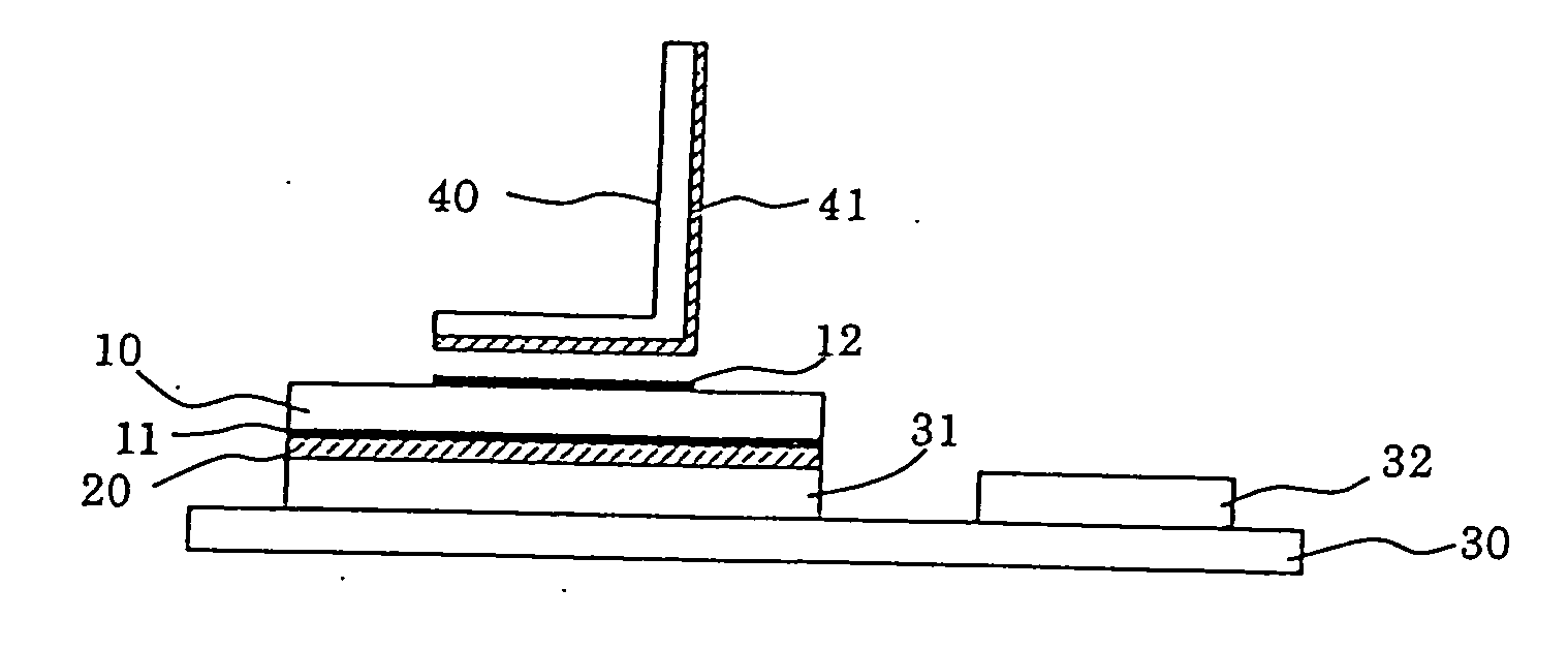
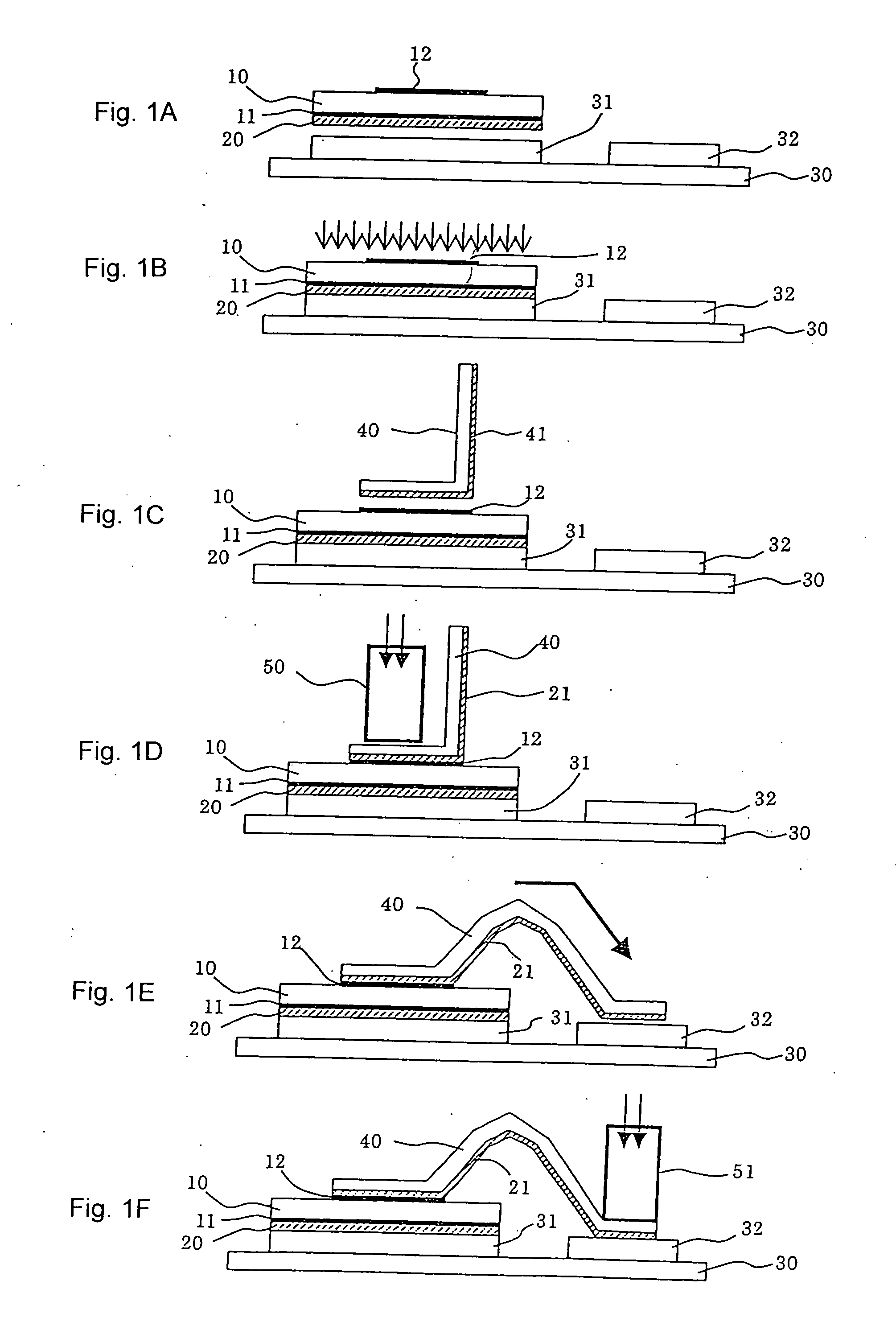
[0154] A following semiconductor module is manufactured in accordance with the steps shown in FIG. 1.

[0155] First of all, an IGBT die is used as the semiconductor die. On the semiconductor die, as the front-surface-die electrode and the back-surface-die electrode, a three-layered electrode which is made of Ti / Ni / Au and has an Au layer on a topmost surface thereof is formed.

[0156] On the other hand, on an Al-base insulation circuit board made of Al as a base material, an electrode made of Cu and having a thickness of 0.32 mm is formed as the first circuit electrode.

[0157] Then, as the connecting member, a lead frame made of Cu alloy and having a thickness of 0.25 mm is used.

[0158] Next, the low-melting-point metal layer made of SnIn (melting point: 117° C.) and having a thickness of 5 μm is formed on the back-surface-die electrode by sputtering, and the low-melting-point metal layer made of SnIn (melting point: 117° C.) and having a thickness of 5 μm is formed on the whole surfac...

example 2

[0163] The semiconductor module is manufactured under the same conditions as the example 1 except for the following. That is, in the example 1, the low-melting-point metal layer having a total thickness of 1 μm is formed by sequentially stacking a Sn layer made of a single metal layer and having a thickness of 0.48 μm and an In layer made of a single metal layer and having a thickness of 0.52 μm using sputtering. In the respective first to third steps, the preheating is performed at a temperature of 120° C. for 10 seconds, and the Sn layer and the In layer are formed into the solid solution thus obtaining a SnIn alloy layer. Thereafter, the first to third joining steps are performed.

[0164] Accordingly, in this example 2, in the same manner as the example 1, it is also possible to manufacture the semiconductor module at a temperature equal to or below 200° C. without soldering.


PUM


Abstract

The present invention provides a manufacturing method of a semiconductor module which enables the joining at a low temperature within a short time and can obtain more reliable joining portions by performing the joining without using a solder joining medium. The manufacturing method of a semiconductor module includes a first joining step for joining first circuit electrodes which are formed on a circuit board and back-surface-side die electrodes of a semiconductor die, a second joining step for joining the front-surface-side electrodes of the semiconductor die and one ends of lead frames, and a third joining step for joining another ends of the lead frame and second circuit electrodes which are formed on the circuit board, wherein a low-melting-temperature metal layer is formed on one conductive portion of a pair of conductive portions to be joined and, thereafter, the low-melting-temperature metal layer is heated and pressurized thus diffusing the low-melting-temperature metal layer into the pair of conductive portions by solid-liquid diffusion whereby the conductive portions are joined to each other.

Description

TECHNICAL FIELD [0001] The present invention relates to, for example, a manufacturing method of a semiconductor module such as a power semiconductor using a lead frame and aluminum wire bonding. BACKGROUND ART [0002] A power conductor is a large-capacity semiconductor which exhibits a voltage or a current larger than a voltage or a current used in a semiconductor for a personal computer or the like and has been popularly used in an electric power field, rail roads, automobiles, household electric appliances and the like, [0003] Among modules which use such a power semiconductor, in a module-of a power transistor semiconductor of a general-purpose inverter having a capacitance of 0.1 kW to 5.5 kW which is used as a control device for various motors, power transformers or the like, a lead frame made of copper alloy has been conventionally used to decrease an electric resistance value of wiring and, at the same time, to obtain the excellent thermal characteristics. [0004]FIG. 4 shows o...

Claims


Application Information

Patent Timeline
IPC IPC(8): H01L21/44H01L21/60H01L23/495
CPCH01L23/49562H01L24/33H01L24/36H01L24/40H01L24/45H01L24/48H01L24/83H01L24/84H01L2224/45124H01L2224/48091H01L2224/48472H01L2224/48699H01L2224/73265H01L2224/83191H01L2224/83801H01L2924/01004H01L2924/01005H01L2924/01006H01L2924/01013H01L2924/01014H01L2924/01015H01L2924/01022H01L2924/01028H01L2924/01029H01L2924/0103H01L2924/01032H01L2924/01047H01L2924/0105H01L2924/01051H01L2924/01078H01L2924/01079H01L2924/01082H01L2924/01083H01L2924/01088H01L2924/01322H01L2924/014H01L2924/13055H01L2924/30105H01L2224/32225H01L2924/01019H01L2924/01033H01L2924/0132H01L2224/45032H01L2924/157H01L2224/29109H01L2224/29111H01L2224/29113H01L2224/48227H01L2224/83825H01L2224/84825H01L2924/1305H01L2924/00014H01L2924/01049H01L2924/00015H01L2924/00012H01L2924/00H01L2924/351H01L2924/15787H01L2224/40225H01L2224/40095H01L2224/37147H01L24/37H01L2224/05639H01L2224/05644H01L2224/05655H01L2224/05647H01L24/77H01L2224/37032H01L2224/73221
Inventor FUJIMOTO, KOZOWATANABE, HIROHIKOIKEMI, KAZUTAKAMATSUMURA, KEIICHISHIMODA, MASAYOSHITANIGUCHI, KATSUMIGOTO, TOMOAKI
Owner FUJI ELECTRIC CO LTD
Why Eureka
Try Eureka