Method for manufacturing semiconductor device

a manufacturing method and semiconductor technology, applied in the direction of sustainable manufacturing/processing, final product manufacturing, instruments, etc., can solve the problems of low yield, difficult to manufacture thin film transistors, memory and solar cells having fine structures, and difficult to achieve the reduction in size and weight, and achieve the improvement of performance of semiconductor devices. , the effect of high yield and easy manufacturing

Inactive Publication Date: 2007-09-06
SEMICON ENERGY LAB CO LTD
View PDF26 Cites 84 Cited by
  • Summary
  • Abstract
  • Description
  • Claims
  • Application Information

AI Technical Summary

Benefits of technology

[0020]In the present invention, a photocatalytic layer and an organic compound layer are formed over a substrate having a light transmitting property, an element forming layer having an element with a fine structure is formed over the photocatalytic layer and the organic compound layer by using a semiconductor process, and then, the photocatalytic layer is irradiated with light from the substrate having the light transmitting property. Accordingly, at an interface between the photocatalytic layer and the organic compound layer, photocatalytic reaction can be generated and the photocatalytic layer and the organic compound layer can be separated from each other without using light with high energy. Therefore, a semiconductor device which has flexibility and an element including a fine structure formed by using a conventional semiconductor process can be easily manufactured. In addition, a semiconductor device which has flexibility and an element forming layer including an element with a fine structure can be manufactured with high yield by using a conventional semiconductor process.
[0021]In addition, after a photocatalytic layer, an organic compound layer having a light shielding property, and an element forming layer are sequentially formed over a substrate having a light transmitting property, the photocatalytic layer is irradiated with light from the substrate having the light transmitting property, and the photocatalytic layer and the organic compound layer having the light shielding property can be separated from each other. At this time, light with which the photocatalytic layer is irradiated can be prevented from entering the element forming layer; therefore, a characteristic of the element can be prevented from changing due to light, and a semiconductor device which has high reliability and flexibility can be manufactured. In addition, a semiconduct

Problems solved by technology

Therefore, a problem of aligning the metal mask leads to low yield.
Thus, it is difficult to manufacture thin film transistors, memories, and solar cells having fine structures, or the like, and thus it is difficult to achieve reduction in size and weight and improvement in performance of semiconductor devices.
In the separation method shown in Reference 2, a laser beam is delivered from a glass substrate side to peel a polyimide layer; however, th

Method used


Image

  • Method for manufacturing semiconductor device
  • Method for manufacturing semiconductor device
  • Method for manufacturing semiconductor device

Examples


embodiment mode 1

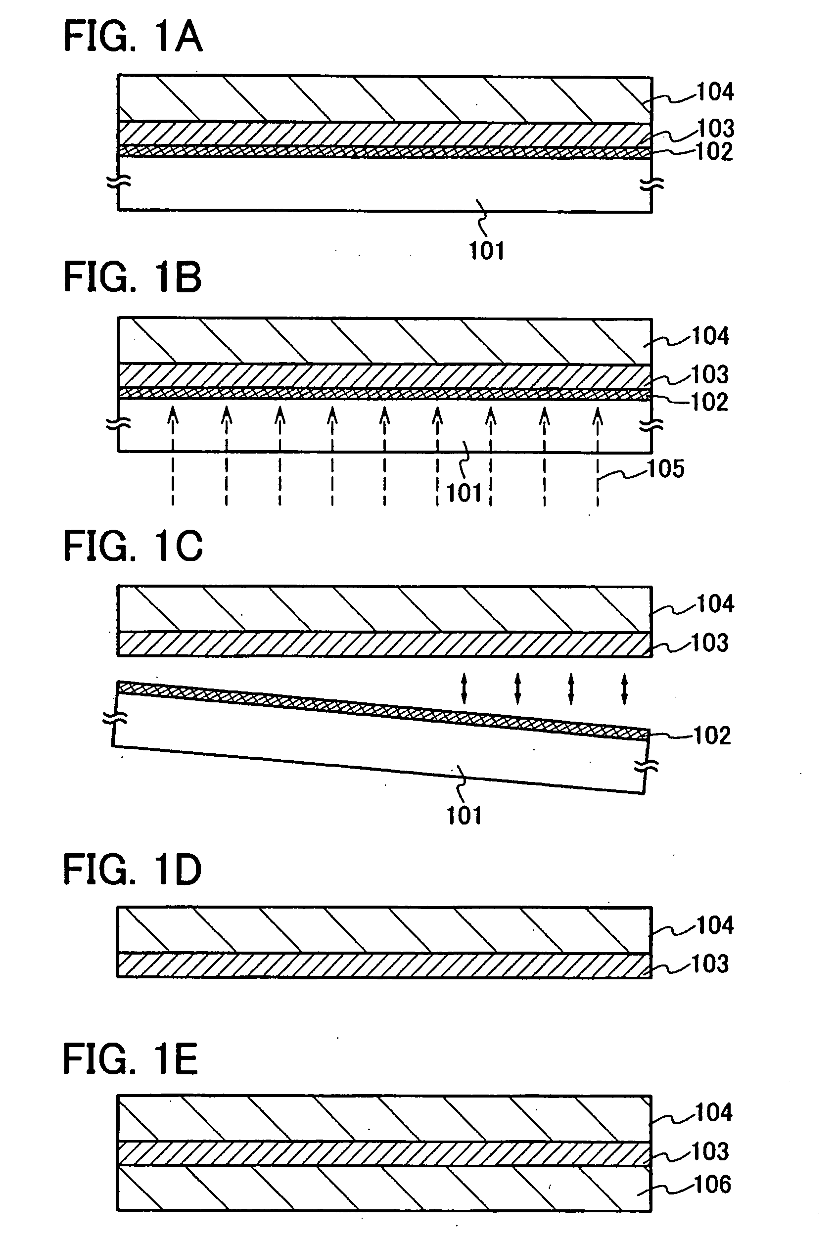
[0059]This embodiment mode will describe a method for manufacturing a semiconductor device having flexibility with high yield by separating an element forming layer from a substrate having a light transmitting property, with reference to FIGS. 1A to 1E.

[0060]As shown in FIG. 1A, a photocatalytic layer 102 is formed over a substrate 101 having a light transmitting property, and an organic compound layer 103 is formed over the photocatalytic layer 102. Next, an element forming layer 104 is formed over the organic compound layer 103.

[0061]As the substrate 101 having the light transmitting property, a glass substrate, a quartz substrate, a plastic substrate having heat resistance enough to withstand the process temperature of the process, or the like can be used. Since the above-mentioned substrate 101 having a light transmitting property is not restricted in size and shape, for example, a rectangular substrate with a length of 1 m or more on a side can be used as the substrate 101 havi...

embodiment mode 2

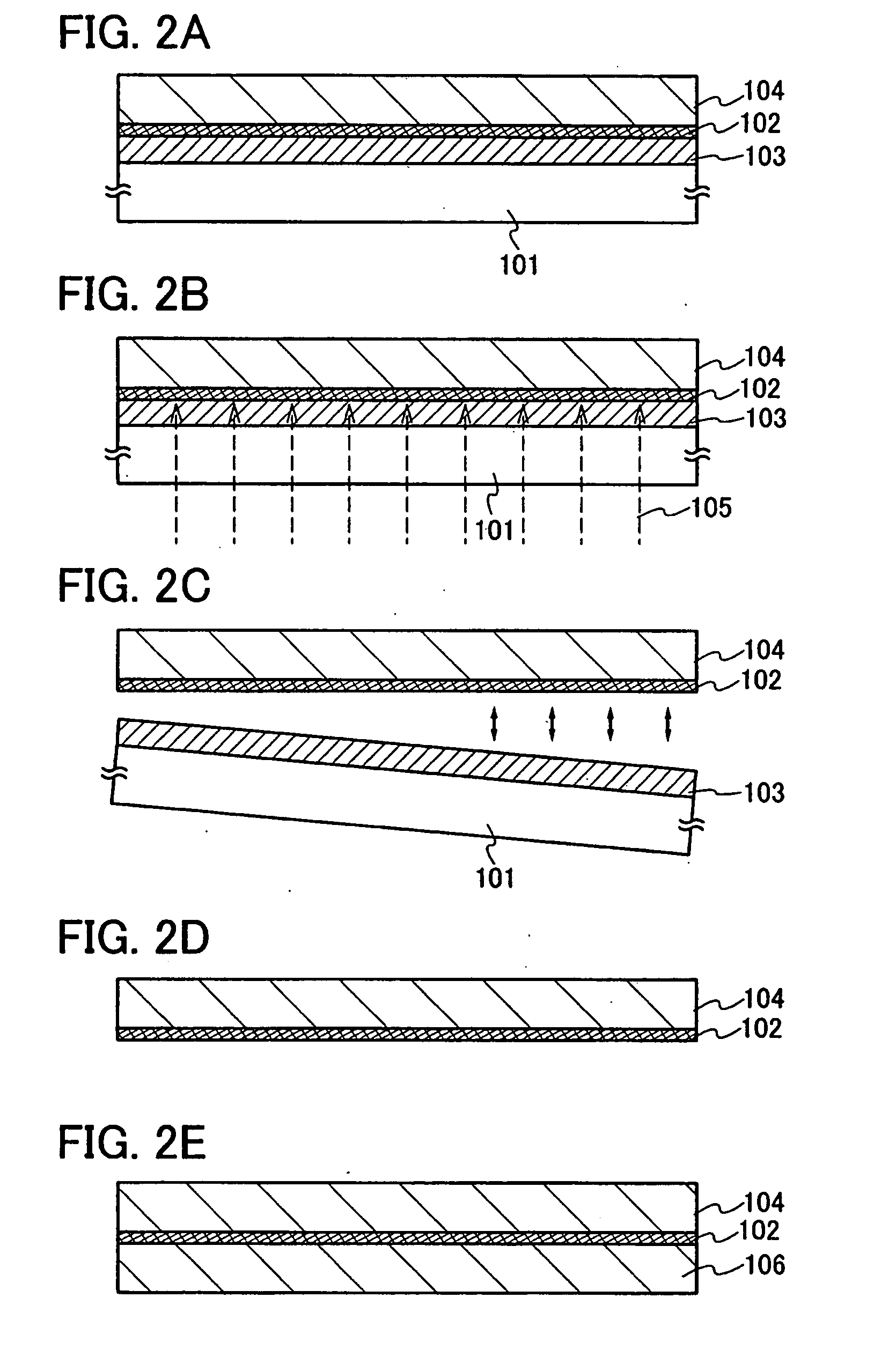
[0074]This embodiment mode will describe another mode of a manufacturing process of the photocatalytic layer 102 and the organic compound layer 103, which is different from Embodiment Mode 1, with reference to FIGS. 2A to 2E.

[0075]As shown in FIG. 2A, the organic compound layer 103 is formed over the substrate 101 having the light transmitting property, and the photocatalytic layer 102 is formed over the organic compound layer 103. Then, the element forming layer 104 is formed over the photocatalytic layer 102.

[0076]In this embodiment mode, since the photocatalytic layer 102 is irradiated with light through substrate 101 having a light transmitting property and the organic compound layer 103, the organic compound layer 103 is formed using a material capable of transmitting light which is to be delivered later. Typically, a material capable of transmitting any of ultraviolet rays, visible rays, or infrared rays is used. As an organic compound having a light transmitting property, the...

embodiment mode 3

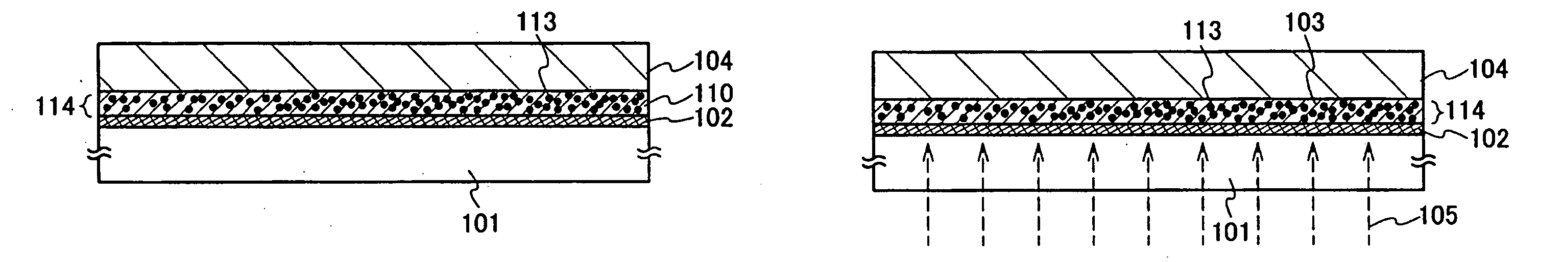
[0080]This embodiment mode will describe a mode in which a semiconductor device is formed using an organic compound layer 112 in which inorganic compound particles are dispersed instead of the organic compound layer 103 in Embodiment Modes 1 and 2, with reference to FIGS. 3A to 3E. Note that in this embodiment mode, Embodiment Mode 1 is used for description; however, Embodiment Mode 2 can be applied.

[0081]As shown in FIG. 3A, the photocatalytic layer 102 is formed over the substrate 101 having the light transmitting property, and the organic compound layer 112 is formed over the photocatalytic layer 102. Then, the element forming layer 104 is formed over the organic compound layer 112. Note that as the organic compound layer 112, inorganic compound particles 111 are dispersed in an organic compound 110.

[0082]As the inorganic compound particles 111, silicon oxide, silicone nitride, aluminum oxide, tantalum oxide, barium fluoride magnesium, or the like can be used. When the inorganic ...


PUM

PropertyMeasurementUnit
Flexibilityaaaaaaaaaa
Wavelengthaaaaaaaaaa
Lightaaaaaaaaaa

Abstract

A method for manufacturing a semiconductor device includes: forming a photocatalytic layer and an organic compound layer in contact with the photocatalytic layer over a substrate having a light transmitting property; forming an element forming layer over the substrate having the light transmitting property with the photocatalytic layer and the organic compound layer in contact with the photocatalytic layer interposed therebetween; and separating the element forming layer from the substrate having the light transmitting property after the photocatalytic layer is irradiated with light through the substrate having the light transmitting property.

Description

BACKGROUND OF THE INVENTION[0001]1. Field of the Invention[0002]The present invention relates to a method for manufacturing a semiconductor device having flexibility.[0003]2. Description of the Related Art[0004]It has been required to manufacture semiconductor devices at low cost, and development of elements such as thin film transistors, memories, and solar cells for control circuits, memory circuits, or the like has been extensively carried out in recent years (for example, Reference 1: Japanese Published Patent Application No. 2004-47791).[0005]Various applications of semiconductor devices having elements such as thin film transistors, memories, and solar cells are expected, and using flexible plastic films is attempted in pursuit of reduction in size and weight.[0006]Since plastic films have low heat resistance, it is necessary to decrease the highest temperature in a process. Therefore, a method for manufacturing a semiconductor element is limited. Accordingly, the semiconducto...

Claims


Application Information

Patent Timeline
IPC IPC(8): H01L21/00G02F1/167
CPCH01L27/1214H01L27/1266H01L27/3244H01L29/78603H01L29/78633Y02E10/549H01L51/003H01L51/56H01L2227/326H01L2251/5338H01L31/0392H01L31/03925H01L31/03926H01L27/1218G02F1/167Y02P70/50H10K59/12H10K71/80H10K59/1201H10K2102/311H10K71/00H10K10/00H10K59/126G02F1/133305G02F1/133345G02F1/133711G02F1/133734G02F1/133784G02F1/13394H01L31/1896
Inventor MORISUE, MASAFUMIJINBO, YASUHIROFUJII, GENKIMURA, HAJIME
Owner SEMICON ENERGY LAB CO LTD
Why Eureka
Try Eureka