Unlock instant, AI-driven research and patent intelligence for your innovation.
Metrology System of Fine pattern for Process Control by Charged Particle Beam
Inactive Publication Date: 2007-09-27
HITACHI HIGH-TECH CORP
View PDF5 Cites 15 Cited by
Summary
Abstract
Description
Claims
Application Information
AI Technical Summary
This helps you quickly interpret patents by identifying the three key elements:
Problems solved by technology
Method used
Benefits of technology
Benefits of technology
[0009]The object of the present invention is to address the above-mentioned problem and provide a charged particle beam pattern measurement technique that makes possible a high-accuracy measurement with high throughput at all measurement points.
[0029]According to the present invention, it becomes possible to perform measurement and inspection of the fine pattern by the charged particle beam with high throughput.
Problems solved by technology
However, if a surface potential estimated beforehand contains a large error or if rotational symmetry of the in-plane distribution of the surface potential of the sample is low, it will take time to adjust a retarding voltage, which will cause throughput of a metrologysystem to be reduced.
Moreover, regarding astigmatism, simple impression of the corrected retarding voltage has no effect at all, and the problem remains not solved.
As described above, the conventional method for measuring a fine pattern using a CD-SEM bears a problem that the throughput lowers for a charged-up sample.
Method used
Image
Click on the blue label to locate the original text in one second.
Reading with bidirectional positioning of images and text.
Examples
first embodiment
[0052]In a first embodiment of the present invention, a soft x-ray irradiator is installed on a transportation path of a sample and simultaneously at a position in the atmosphere, whereby regarding inspection of a charged-up sample, a measurement with the same accuracy and the same throughput as those of a non-charged up sample becomes possible.
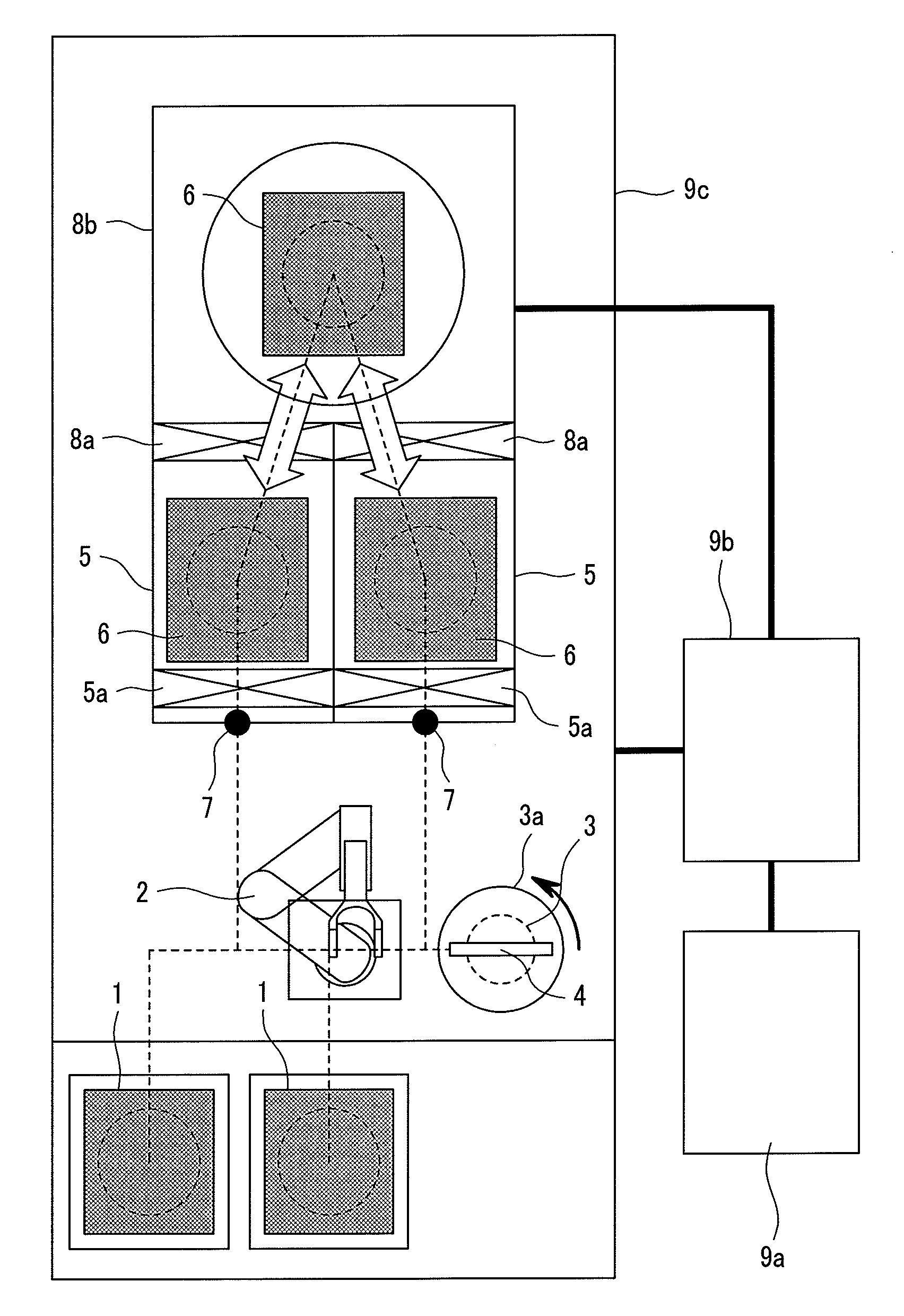
[0053]FIG. 1A shows the first embodiment of the present invention, specifically showing a sample introduction unit of a metrologysystem of fine pattern using an electron beam. Hereafter, a metrology system will be explained by taking a semiconductorwafer being a sample as an example.
[0054]A command to inspect a predetermined wafer in the wafer cassette 1 in FOUP (Front Opening Unified Pod) or SMIF (Front Opening Unified Pod) is inputted. A predetermined wafer is automatically taken out by a mechanical arm 2 for wafer transportation of an atmosphere-side robot. In the figure, two wafer cassettes can be carried by a load board section. It is ...
second embodiment
[0069]In a second embodiment of the present invention, a soft x-ray irradiator is installed on the transportation path and in the atmosphere, whereby also regarding inspection of a charged-up sample, a measurement with the same throughput as that of the non-charged up sample becomes possible.
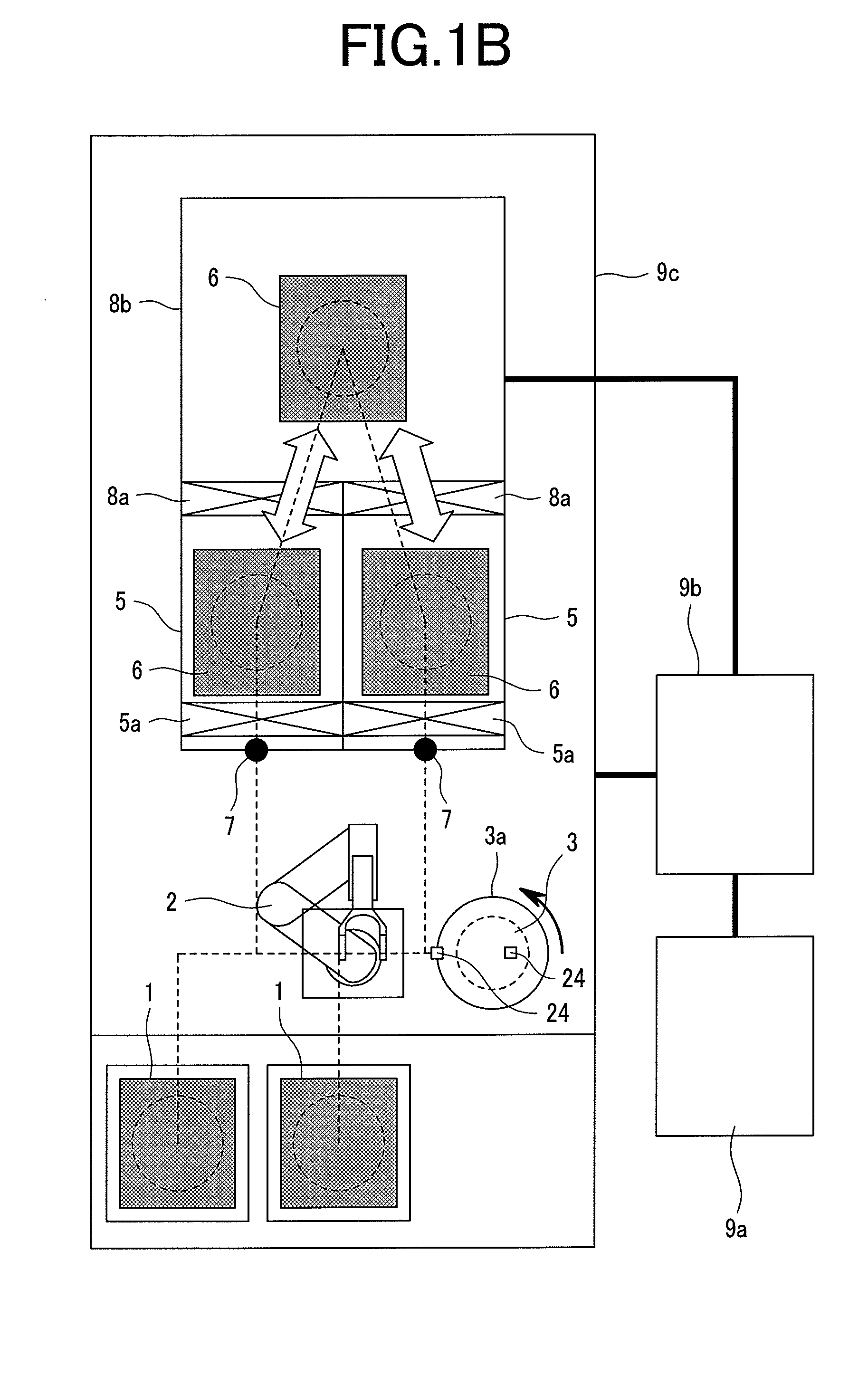
[0070]FIG. 1B shows the second embodiment of the present invention, specifically showing a sample introduction unit of a metrology system of fine pattern using an electron beam. Hereafter, taking a sample of a semiconductor wafer as a sample, this embodiment will be explained.
[0071]A wafer is taken out from a wafer cassette 21 in FOUP or SMIF by a mechanical arm 22 for wafer transportation of the atmosphere-side robot. Although according to the figure, two wafer cassettes can be carried, it is possible that they are specified to be cassettes of the same wafer size or cassettes of different forms. The taken out wafer is temporarily transported to a rotation stage 23 by the mechanical arm 22 for w...
third embodiment
[0083]In a third embodiment of the present invention, one or more electrodes are arranged on the transportation path of the sample, whereby length measurementprocessing with an equivalent throughput to that of the non-charged up sample becomes possible even in measuring lengths of the charged-up sample.
[0084]FIG. 6 shows the third embodiment of the present invention, specifically showing a sample introduction unit of a metrology system using an electron beam. Hereafter, taking a semiconductor wafer as an example, the embodiment will be explained.
[0085]Like the case of the second embodiment, a wafer is taken out from the wafer cassette 1 currently kept in the FOUP or SMIF by the mechanical arm 2 for wafer transportation of the atmosphere-side robot. The taken-out wafer is temporarily transported to the rotation stage 3 by the mechanical arm 2 for wafer transportation.
[0086]In this embodiment, a plurality of electrodes 64 are arranged as charge neutralizing means right above the rota...
PUM
Abstract
The present invention provides a pattern inspection technique that enables measurement and inspection of a fine pattern by a charged particle beam to be performed with high throughput. A metrologysystem of fine pattern according to the pattern inspection technique has: a the column that includes a charged particle source, an electronoptics for scanning a desired observation area on a sample with a charged particle beam emitted from the charged particle source, and a detector for detecting charged particles generated secondarily from the sample scanned by the charged particle beam; information processing means for measuring information about geometry of a pattern formed on the sample based on information on the intensity of the charged particles obtained by the detector; and a sample introduction unit for introducing the sample into the inside of the column; wherein a charge neutralizer unit for generating ions and charge neutralizing the sample with the ions and surface potential measuring means for measuring a surface potential of the sample surface are provided on a path that is inside the sample introduction unit and transports the sample to the column.
Description
CLAIM OF PRIORITY[0001]The present invention claims priority from Japanese application JP 2006-81456 filed on Mar. 23, 2006, the content of which is hereby incorporated by reference on to this application.BACKGROUND OF THE INVENTION[0002]The present invention relates to a technique for measuring geometry of a fine pattern on the surface of a sample (a semiconductorwafer, a reticle, etc.) and its dimensions.[0003]Currently, the use of a critical-dimension scanning electron microscope (hereinafter abbreviated to as CD-SEM) is a mainstream in measuring dimensions of a semiconductor device pattern. The structure of the CD-SEM is fundamentally the same as that of the scanning electron microscope. First, electrons emitted from an electron source of a heating type or field emission type are accelerated. Subsequently, an electron beam is converged in diameter by a lens to form a focused electron beam. Then, the electron beam is scanned on a sample (e.g., a wafer, a reticle, etc.) and gener...
Claims
Application Information
Patent Timeline
Application Date:The date an application was filed.
Publication Date:The date a patent or application was officially published.
First Publication Date:The earliest publication date of a patent with the same application number.
Issue Date:Publication date of the patent grant document.
PCT Entry Date:The Entry date of PCT National Phase.
Estimated Expiry Date:The statutory expiry date of a patent right according to the Patent Law, and it is the longest term of protection that the patent right can achieve without the termination of the patent right due to other reasons(Term extension factor has been taken into account ).
Invalid Date:Actual expiry date is based on effective date or publication date of legal transaction data of invalid patent.

