Resist composition, method for forming resist pattern, and semiconductor device and method for manufacturing the same

a technology of resist composition and pattern, which is applied in the direction of photosensitive materials, instruments, photomechanical equipment, etc., can solve the problems of high cost, arf excimer, and difficulty in developing resist materials suitable for short wavelength exposure, etc., to achieve efficient and uniform thickening, improve the effect of reducing the risk of arc excimer, and exceeding the exposure or resolution limi

Inactive Publication Date: 2007-09-27
FUJITSU LTD
View PDF10 Cites 36 Cited by
  • Summary
  • Abstract
  • Description
  • Claims
  • Application Information

AI Technical Summary

Benefits of technology

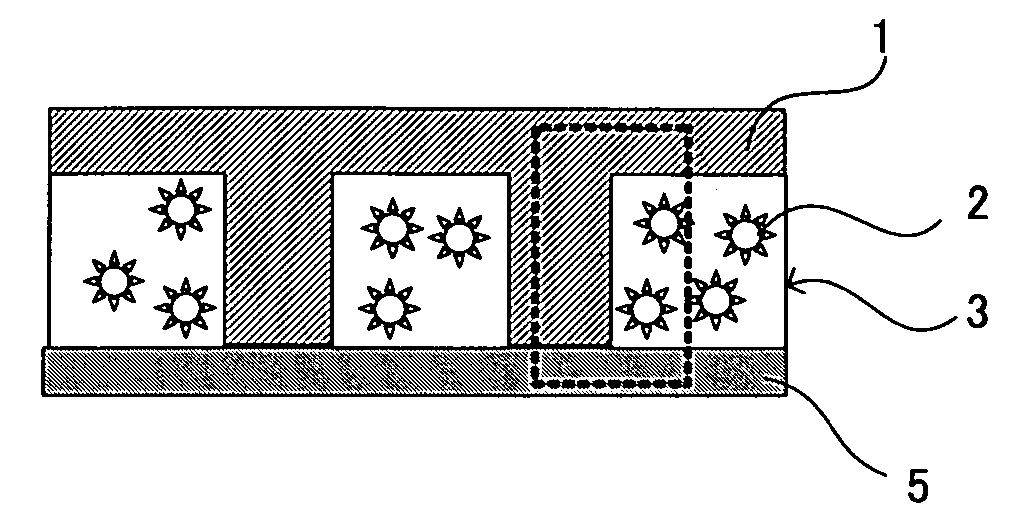
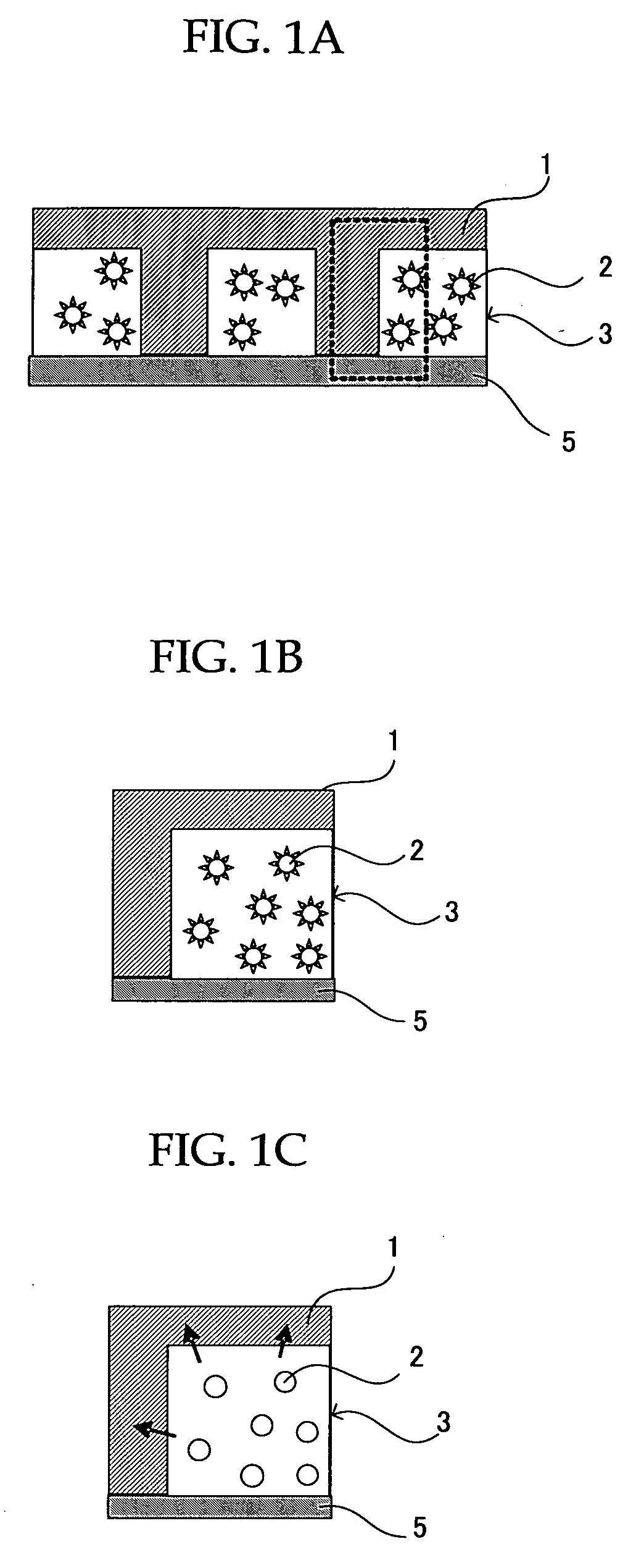
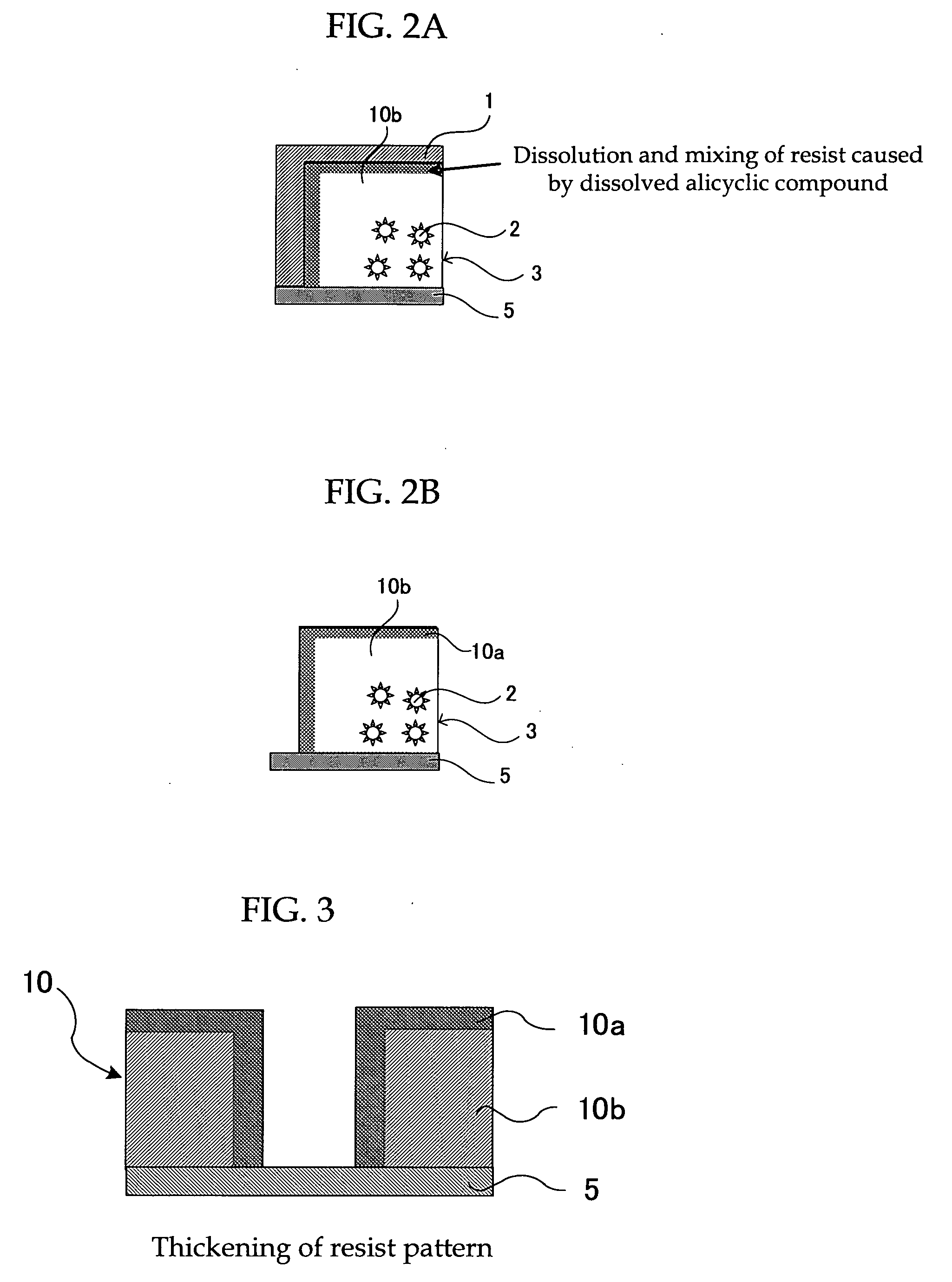
[0024] In the method for forming a semiconductor device of the present invention, a resist pattern is formed from the resist composition of the invention on a surface of a workpiece serving as a subject on which interconnection patterns, etc., are formed, and then the resist pattern thickening material is applied over the resist pattern so as to cover the surface of the resist pattern. When the resist pattern is heated at a temperature near the melting point of the alicyclic compound, 90° C. to 150° C., the alicyclic compound dispersed in the resin in the resist pattern is dissolved. The dissolved alicyclic compound dissolves the resist composition in the resist pattern to thereby cause an interaction or mixing between the alicyclic compound, the resin, and the resist pattern thickening material. Thus, a surface layer or mixing layer, where the resist pattern thickening material and the resist pattern are mixed, is formed on the surface of the resist pattern as the inner layer. In this way, the resist pattern is uniformly thickened with the resist pattern thickening material. Thus, the space pattern formed by use of the thickened resist pattern has a fine structure, exceeding exposure or resolution limits. Since the resist pattern thickening material contains the alicyclic compound, the resist pattern formed from the resist composition is efficiently and uniformly thickened, regardless of the direction and / or spacing variations of the resist pattern, and without depending on components of the like of the resist pattern thickening material, and the thickened amount of the resist pattern has less dependency on the direction and / or spacing variations of the resist pattern, components of the resist pattern thickening material, and the like. Thus, thickened resist patterns such as a space pattern can be easily and precisely formed on an interconnection layer of LOGIC LSI where not only a contact hole pattern, but also various sizes of resist patterns are utilized.
[0025] Subsequently, by etching the surface of the workpiece using the thickened resist pattern as a mask, the surface of the workpiece is patterned finely and precisely with accurate dimension, thus high-quality and high performance semiconductor devices can be produced efficiently having an interconnection pattern with fine, precise, and accurate dimension.
[0026] The semiconductor device of the present invention is manufactured by the method for manufacturing a semiconductor device of the present invention. The semiconductor device has patterns, for example, interconnection patterns, with fine, precise, and accurate dimension, and is of high quality and of high performance.

Problems solved by technology

However, in order to make a light source of an exposure device be a short wavelength, it is necessary to improve the exposure device, which results in very high costs.
Further, the development of new resist materials suitable for an exposure with light of short wavelength is not easy.
In the RELACS technique, however, there are the following problems.
An aromatic ring contained in the aromatic resin composition allows KrF excimer laser light (wavelength: 248 nm) to pass through, but absorbs ArF excimer laser light (wavelength: 193 nm) having a shorter wavelength than the KrF excimer laser light and does not allow the ArF excimer laser light to pass through.
Therefore, when the KrF resist is used, ArF excimer laser light cannot be used as the exposure light, which makes it impossible to from a fine interconnection pattern, etc.
Moreover, there is a problem in the RELACS technique that the resist swelling material is effective in thickening or swelling the KrF resist, however, ineffective in thickening or swelling the ArF resist.
When an x-ray or electron beam having a shorter wavelength than the ArF excimer laser light is applied as exposure light to form the pattern, however, it results in high cost and low productivity.
As mentioned above, in the RELACS technique, the aforementioned resist swelling material does not efficiently work on ArF resist pattern.
Thus, there was a problem that when the resist pattern thickening material was used for a space pattern, on an interconnection layer of LOGIC LSI where various sizes of resist patterns are used, the burden on designing an exposure mask could not fully be alleviated.
Thus, the current situation is that there has not yet been developed a technique which can use ArF excimer laser light as the light source of an exposure device during patterning, which can sufficiently thicken ArF resist pattern or the like that cannot be thickened by using the aforementioned resist swelling material used in the RELACS technique, and which can easily form a fine space pattern of resist or an interconnection pattern at low cost.

Method used


Image

  • Resist composition, method for forming resist pattern, and semiconductor device and method for manufacturing the same
  • Resist composition, method for forming resist pattern, and semiconductor device and method for manufacturing the same
  • Resist composition, method for forming resist pattern, and semiconductor device and method for manufacturing the same

Examples


example 1

—Preparation of Resist Composition—

[0182] A resist composition having the following composition was prepared.

Resin*1  12 parts by massTriphenylsulfonium nonafluorobutane sulfonate0.48 parts by massTrioctylamine0.01 parts by massNorbornanon*20.12 parts by massSurfactant*30.005 parts by mass Propyleneglycol methyl ether acetate 100 parts by mass

*1resin represented by the following Structural Formula (9) which was synthesized by the method described in Example 13 in the section of Examples of Japanese Patent No. 3297272.

*2norbornanon represented by the following Structural Formula (6), having a melting point of around 95° C.

*3KP-341, available from Shin-Etsu Chemical Co., Ltd.

Structural Formula (9)Structural Formula (6)

—Formation of Resist Pattern—

[0183] The thus prepared resist composition of the present invention was applied over the entire surface of a silicon wafer (available from Mitsubishi Material Corporation) by spin-coating at 3,500 rpm for 20 seconds, and the coated resi...

example 2

[0187] A thickened resist pattern was formed in the same manner as in Example 1 except that the resist pattern thickening material (AZ R500™, available from AZ Electronic Materials) suited for ArF excimer laser light was replaced by a resist pattern thickening material (AZ R600™, available from AZ Electronic Materials) suited for ArF excimer laser light. The variations of the pattern sizes in the narrow side direction and the wide side direction were calculated, respectively. The variations of the pattern size were 30 nm in the narrow side direction and 32 nm in the wide side direction. Accordingly, it was found that the use of the resist composition of the present invention allowed uniformly thickening the resist pattern and without depending on the components of the resist pattern thickening material.

example 3

[0189] A thickened resist pattern was formed in the same manner as in Example 1 except that the resist composition was prepared based on the following composition. The variations of the pattern sizes in the narrow side direction and the wide side direction were measured, respectively.

[0190]—Preparation of Resist Composition—

ArF resist (AX5910, available from Sumitomo Chemical Co., Ltd.)5 g1-adamantylmethanol*13 mg

*11-adamantylmethanol represented by the following Structural Formula (1), having a melting point of around 115° C.

Note that as the ArF resist (AX5910) is a commercially available product, the exact concentration of the resin is unknown, however, the content of 1-adamantylmethanol to the mass of the base resin is estimated to be around 0.5% by mass.

Structural Formula (1)

—Formation of Resist Pattern—

[0191] A resist pattern was formed in the same manner as in Example 1, by using the obtained resist composition. Over the surface of the thus obtained resist pattern, a resist...


PUM

PropertyMeasurementUnit
melting pointaaaaaaaaaa
wavelengthaaaaaaaaaa

Abstract

The present invention provides a resist composition which enables uniformly thickening a resist pattern with a resist pattern thickening material, regardless of the direction, spacing variations of the resist pattern, and the components of the resist pattern thickening material and enables forming a fine space pattern of resist, exceeding exposure limits of light sources of exposure devices at low cost, easily, and efficiently. The resist composition contains an alicyclic compound (melting point: 90° C. to 150° C.), and a resin. The method for manufacturing a semiconductor device includes forming a resist pattern on a surface of a workpiece to be processed by using a resist composition and applying a resist pattern thickening material on the surface of the workpiece so as to cover the surface of the resist pattern to thicken the resist pattern; and patterning the surface of the workpiece by etching thereof using the thickened resist pattern as a mask.

Description

CROSS-REFERENCE TO RELATED APPLICATIONS [0001] This application is based upon and claims the benefits of the priority from the prior Japanese Patent Application No. 2006-083173, filed on Mar. 24, 2006, the entire contents of which are incorporated herein by reference. BACKGROUND OF THE INVENTION [0002] 1. Field of the Invention [0003] The present invention relates to a composition used for a resist pattern that is formed in manufacturing a semiconductor device. The present invention also relates to a method for forming a resist pattern which includes forming a fine space pattern of resist, exceeding exposure limits (resolution limits) of light sources of available exposure devices by thickening the resist pattern; a semiconductor device, and a method for manufacturing the semiconductor device. [0004] 2. Description of the Related Art [0005] Semiconductor integrated circuits are becoming more highly integrated, and LSIs and VLSIs are being put into practical use. Accompanying this tr...

Claims


Application Information

Patent Timeline
Patent Type & Authority Applications(United States)
IPC IPC(8): G03C1/00
CPCG03F7/40H01L21/0273H01L21/32139H01L21/31144H01L21/0338Y10S430/106Y10S430/114
Inventor NOZAKI, KOJIKOZAWA, MIWA
Owner FUJITSU LTD
Why Eureka
Try Eureka