Resist pattern thickening material, process for forming resist pattern, and process for manufacturing semiconductor device

a technology of resist pattern and thickening material, which is applied in the direction of photosensitive materials, instruments, auxillary/base layers of photosensitive materials, etc., can solve the problems of high cost, inability to develop resist materials suitable for short wavelength exposure, and inability to use arf excimer laser light as exposure ligh

Inactive Publication Date: 2005-02-10
FUJITSU LTD
View PDF18 Cites 9 Cited by
  • Summary
  • Abstract
  • Description
  • Claims
  • Application Information

AI Technical Summary

Problems solved by technology

However, in order to make a light source of an exposure device be a short wavelength, it is necessary to update the exposure device, which results in very high costs.
Further, the development of new resist materials suitable for an exposure with light of short wavelength is not easy.
There is therefore the problem that ArF excimer laser light cannot be used as the exposure light.
Moreover, there is a problem in the RELACS technique that the resist swelling agent is effective for thickening (swelling) the KrF resist but not for thickening (swelling) the ArF resist.
In case x-ray or

Method used


Image

  • Resist pattern thickening material, process for forming resist pattern, and process for manufacturing semiconductor device
  • Resist pattern thickening material, process for forming resist pattern, and process for manufacturing semiconductor device
  • Resist pattern thickening material, process for forming resist pattern, and process for manufacturing semiconductor device

Examples


example 1

-Preparation of Resist Pattern Thickening Material-

Resist pattern thickening materials A-I of the present invention having the compositions shown in Table 1 were prepared. Note that, in Table 1, the unit of the values in. parentheses is parts by mass. In the “resin” column, “KW-3” is a polyvinyl acetal resin (manufactured by Sekisui Chemical Co., Ltd.). In the “phase transfer catalyst” column, “tetramethylammonium acetate”, “tetrabutylammonium acetate” and “tetramethylammonium chloride” are obtainable from Sigma-Aldrich Corporation. In the “crosslinking agent” column, “uril” denotes tetramethoxymethylglycol uril. In the “surfactant” column, “PC-6” is a non-ionic surfactant (a polykaryotic phenol surfactant manufactured by Asahi Denka Co, Ltd.) and “TN-80” is a non-ionic surfactant (a primary alcohol ethoxylate surfactant manufactured by Asahi Denka Co., Ltd.). Further, a mixed liquid of pure water (deionized water) and isopropyl alcohol (whose mass ratio was water (deionized wate...

example 2

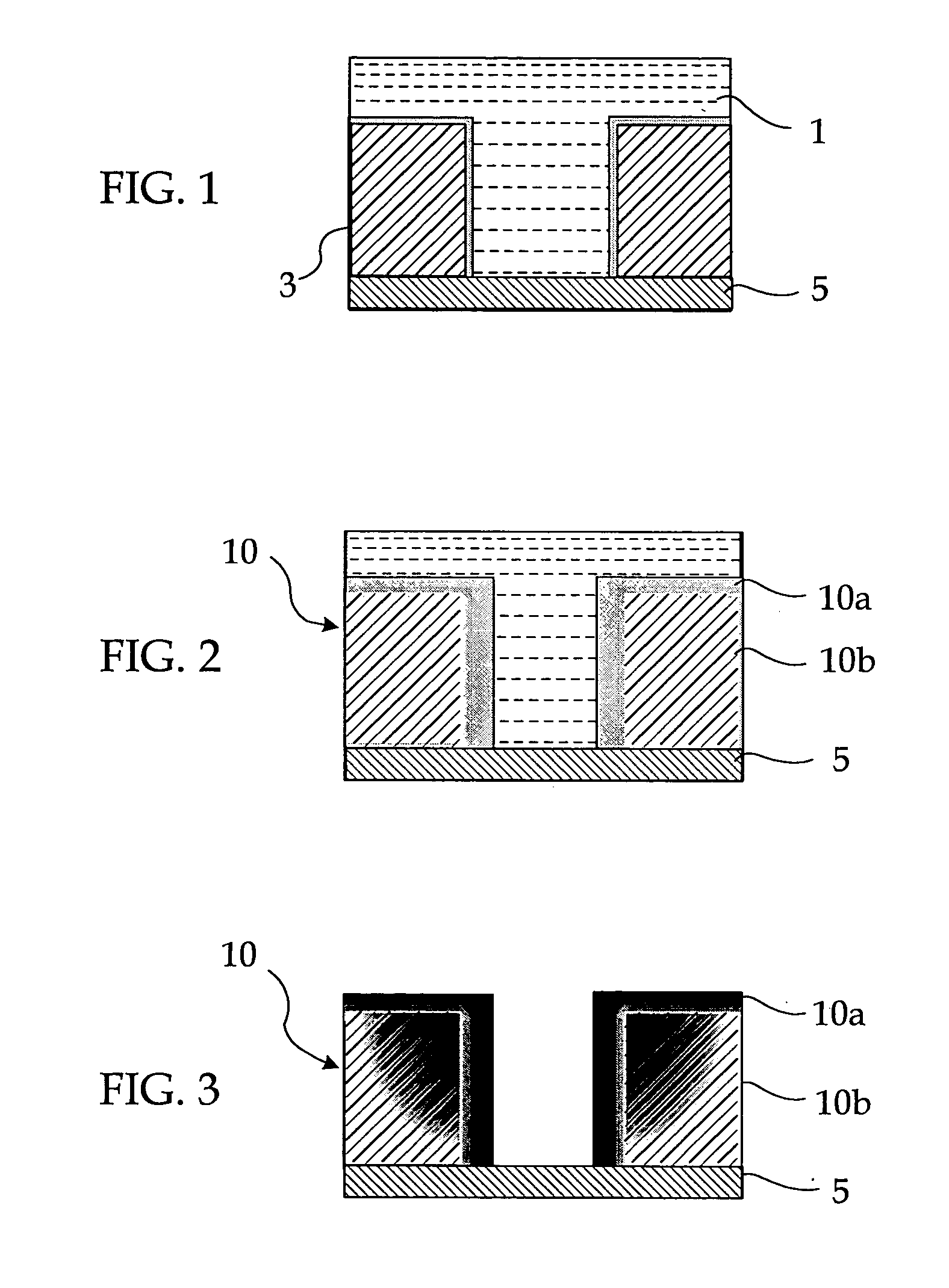
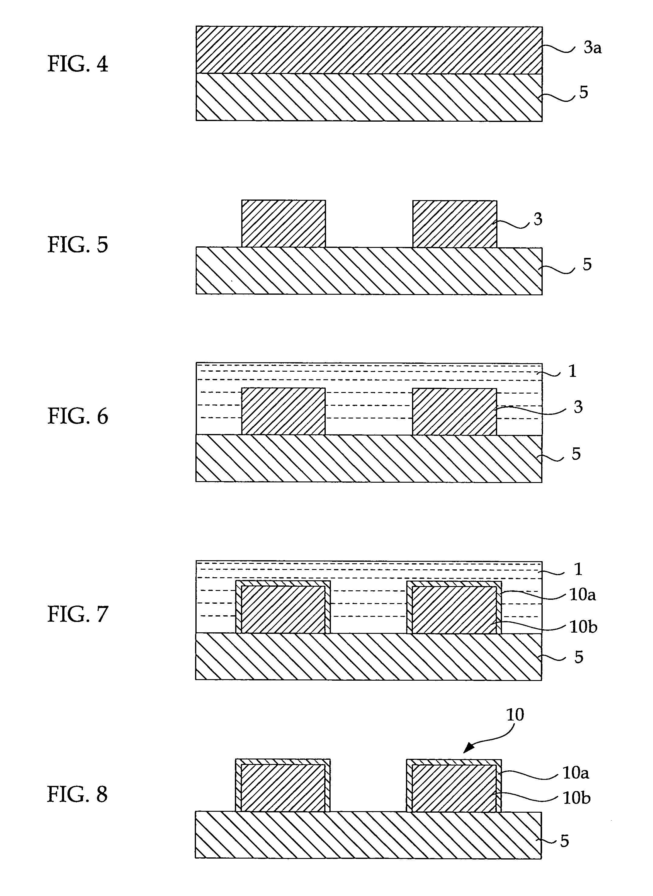
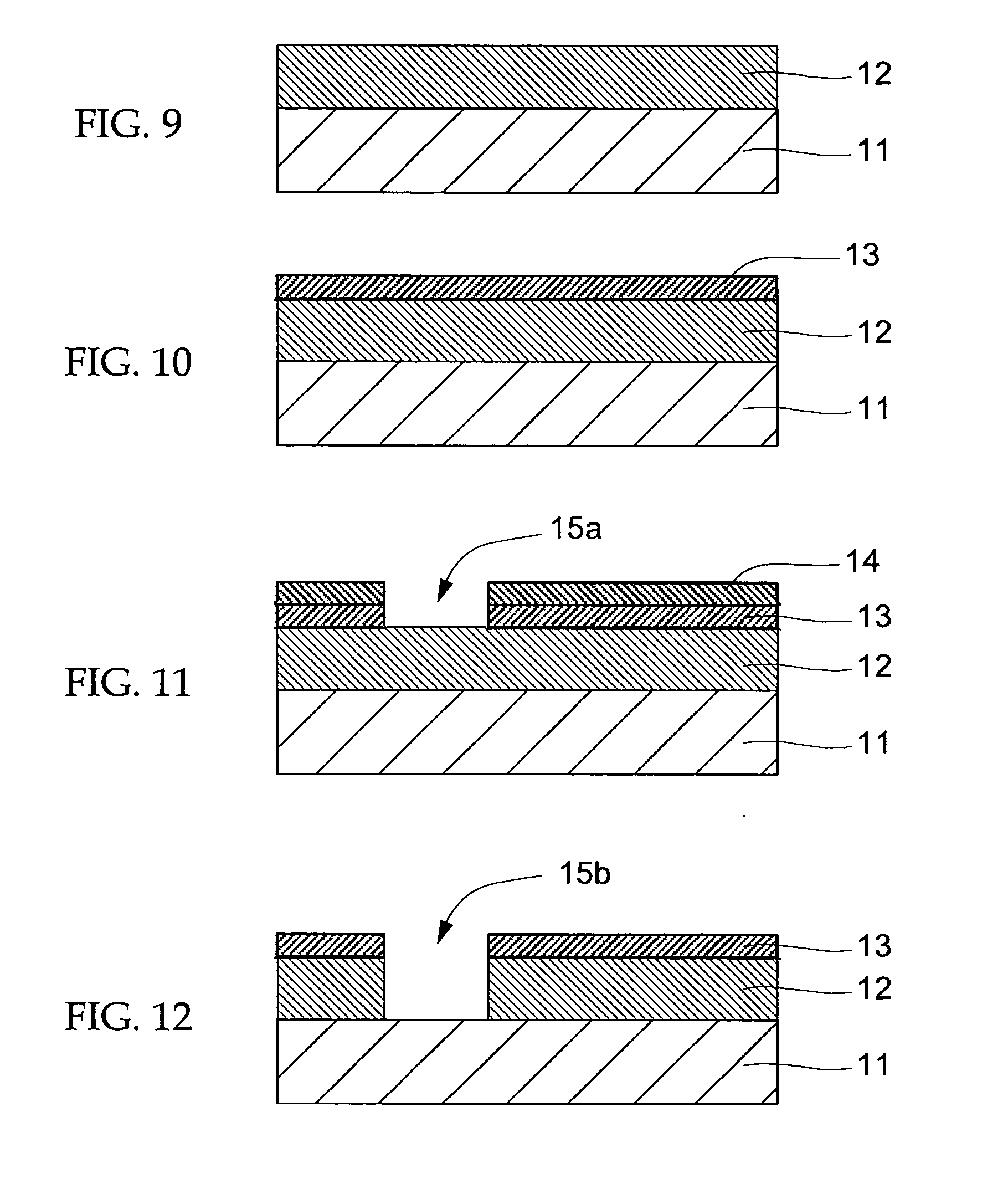
As shown in FIG. 9, an interlayer insulating film 12 was formed on a silicon substrate 11. As shown in FIG. 10, a titanium film 13 was formed by a sputtering method on the interlayer insulating film 12. Next, as shown in FIG. 11, a resist pattern 14 was formed. By using the resist pattern 14 as a mask, the titanium film 13 was patterned by reactive ion etching such that openings 15a were formed. Subsequently, as shown in FIG. 12, the resist pattern 14 was removed by reactive ion etching, and openings 15b were formed in the interlayer insulating film 12 by using the titanium film 13 as a mask.

Next, the titanium film 13 was removed by wet processing, and as shown in FIG. 13, a TiN film 16 was formed on the interlayer insulating film 12 by a sputtering method. Subsequently, a Cu film 17 was grown by an electrolytic plating method on the TiN film 16. Next, as shown in FIG. 14, planarizing was carried out by CMP such that the barrier metal and the Cu film (first metal film) remained o...

example3

-Flash Memory and Process for Manufacturing thereof-

Example 3 is an example of the semiconductor device and process for manufacturing thereof of the present invention using the resist pattern thickening material of the present invention. Note that, in Example 3, resist films 26, 27, 29, and 32 which will be described hereinafter are resist films which have been thickened by the same process as in Examples 1 and 2 by using the resist pattern thickening material of the present invention.

FIGS. 18 and 19 are top views (plan views) of a FLASH EPROM which is called a FLOTOX type or an ETOX type. Note that FIGS. 20 through 28 are cross-sectional schematic views for explaining an example of a process for manufacturing the FLASH EPROM. In FIGS. 20 through 28, the illustrations at the left sides are a memory cell portion (a first element region), and are schematic diagrams of the cross-section (the A direction cross-section) of the gate widthwise direction (the X direction in FIGS. 18 and...


PUM


Abstract

The present invention provides a resist pattern thickening material which can thicken a resist pattern and form a fine space pattern, exceeding exposure limits of exposure light used during patterning. The resist pattern thickening material contains a resin and a phase transfer catalyst. The present invention also provides a process for forming a resist pattern and a process for manufacturing a semiconductor device, wherein the resist pattern thickening material of the present invention is suitably utilized.

Description

BACKGROUND OF THE INVENTION 1. Field of the Invention The present invention relates to a resist pattern thickening material which is applied over a resist pattern to be thickened and is capable of thickening the resist pattern to be thickened, and which can form a fine space pattern, exceeding exposure limits of light sources of existing exposure devices (“space pattern” is hereby defined as a hole, groove, recess, or any other empty space that is formed by a developed (removed) resist). The present invention also relates to a process for forming a resist pattern and a process for manufacturing a semiconductor device, all of which use the resist pattern thickening material. 2. Description of the Related Art Semiconductor integrated circuits are becoming more highly integrated, and LSIs and VLSIs are being put into practical use. Accompanying this trend, the wiring patterns extend to regions of 0.2 μm or less, and the smallest patterns extend to regions of 0.1 μm or less. A litho...

Claims


Application Information

Patent Timeline
IPC IPC(8): H01L21/32G03F7/00G03F7/40G11B5/17G11B5/31H01L21/027H01L21/033H01L21/311H01L21/3213H01L21/8247H01L27/115
CPCG03F7/0035G03F7/40G11B5/17G11B5/313G11B5/3163H01L21/0273H01L27/11543H01L21/0338H01L21/31144H01L21/32139H01L27/115H01L27/11521H01L27/11526H01L21/0337Y10S430/106Y10S430/114H10B69/00H10B41/30H10B41/40H10B41/48H01L21/0332H01L21/0334
Inventor NOZAKI, KOJIKOZAWA, MIWA
Owner FUJITSU LTD
Why Eureka
Try Eureka