Method for wafer level package of sensor chip

a sensor chip and wafer level technology, applied in the direction of semiconductor devices, semiconductor/solid-state device details, electrical devices, etc., can solve the problems of high facility and operation costs, inability to effectively reduce the size of the packaged sensor chip, and the thickness of the final package, so as to reduce the packaging cost

Inactive Publication Date: 2007-09-27
NAT TAIWAN UNIV
View PDF3 Cites 10 Cited by
  • Summary
  • Abstract
  • Description
  • Claims
  • Application Information

AI Technical Summary

Benefits of technology

[0011] The present invention has been made to overcome the aforementioned drawback of packaging methods. The primary object of the present invention is to provide a wafer level package (WLP) method of sensor chips for mass production and reducing the packaging cost.
[0018] The via holes of the present invention can be formed by wet etching (such as, chemical etching), dry etching (such as, reactive ion etching (RIE), inductively coupled plasma reactive ion etching (ICP)), or laser drill. The present invention does not use the special cutting tool required by the U.S. Pat. No. 6,646,289. Therefore, the present invention is simpler, precise, and inexpensive to produce in comparison. In addition, the present invention also avoids the pollution caused by cutting.

Problems solved by technology

As this type of packaging process requires a highly clean environment (Class 100), the costs of the facility and operation are both high.
In addition, as the volume of the packaging structure is sizeable, the size of the packaged sensor chip cannot be effectively reduced.
However, this method has two drawbacks.
The drawbacks of this method include the thickness of the final package, the complexity of the process and the bump is prone to damage.
Its drawbacks include high cost (two glass layers and special cutting tool), difficulty of cutting precision, high error rate, pollution during cutting, and the bump electrode prone to breakage.

Method used


Image

  • Method for wafer level package of sensor chip
  • Method for wafer level package of sensor chip
  • Method for wafer level package of sensor chip

Examples


Embodiment Construction

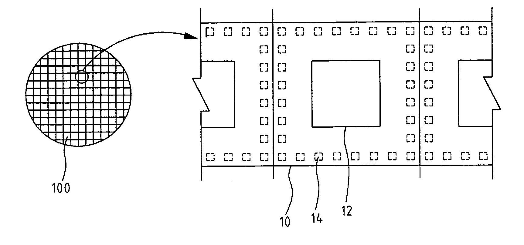
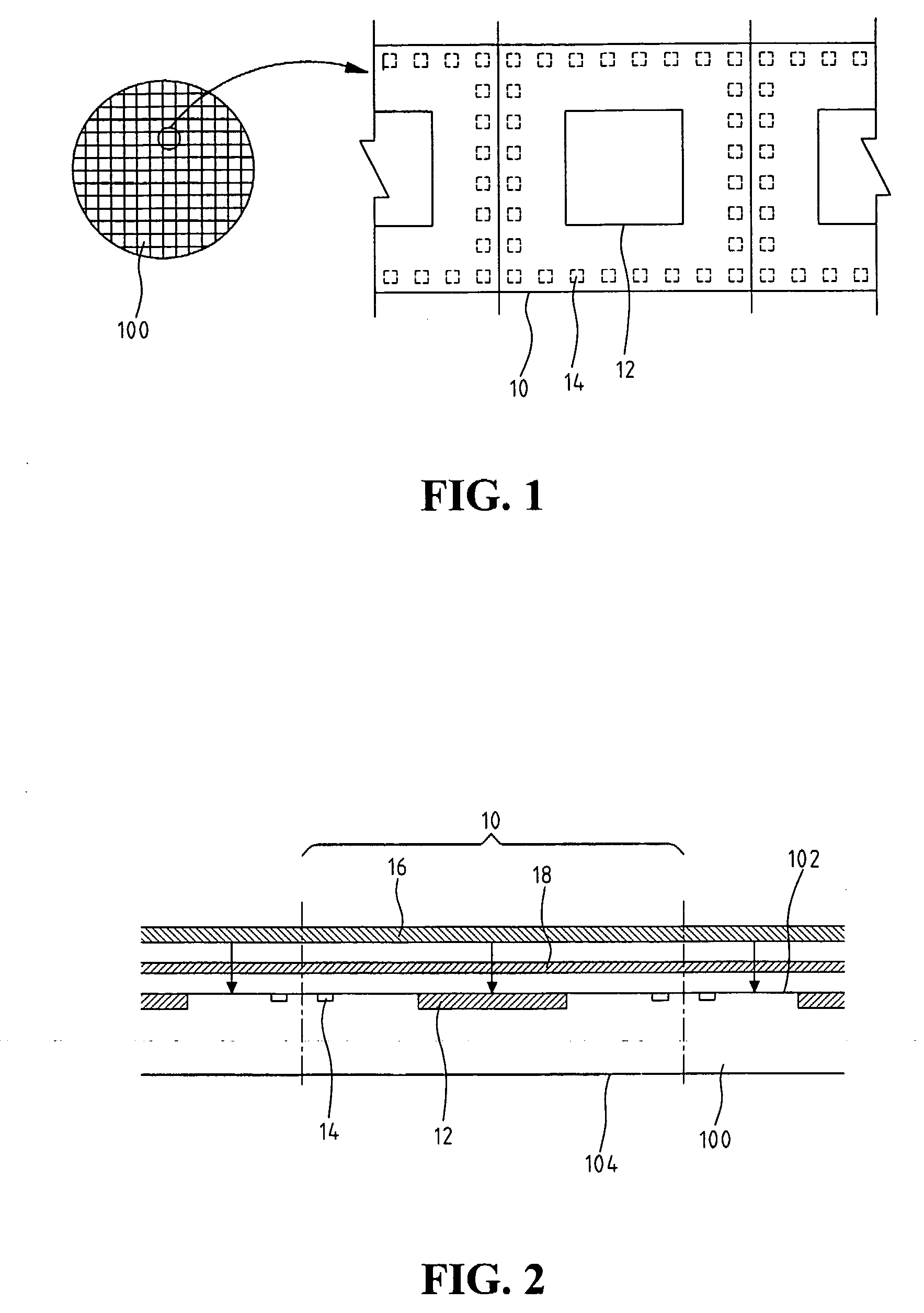
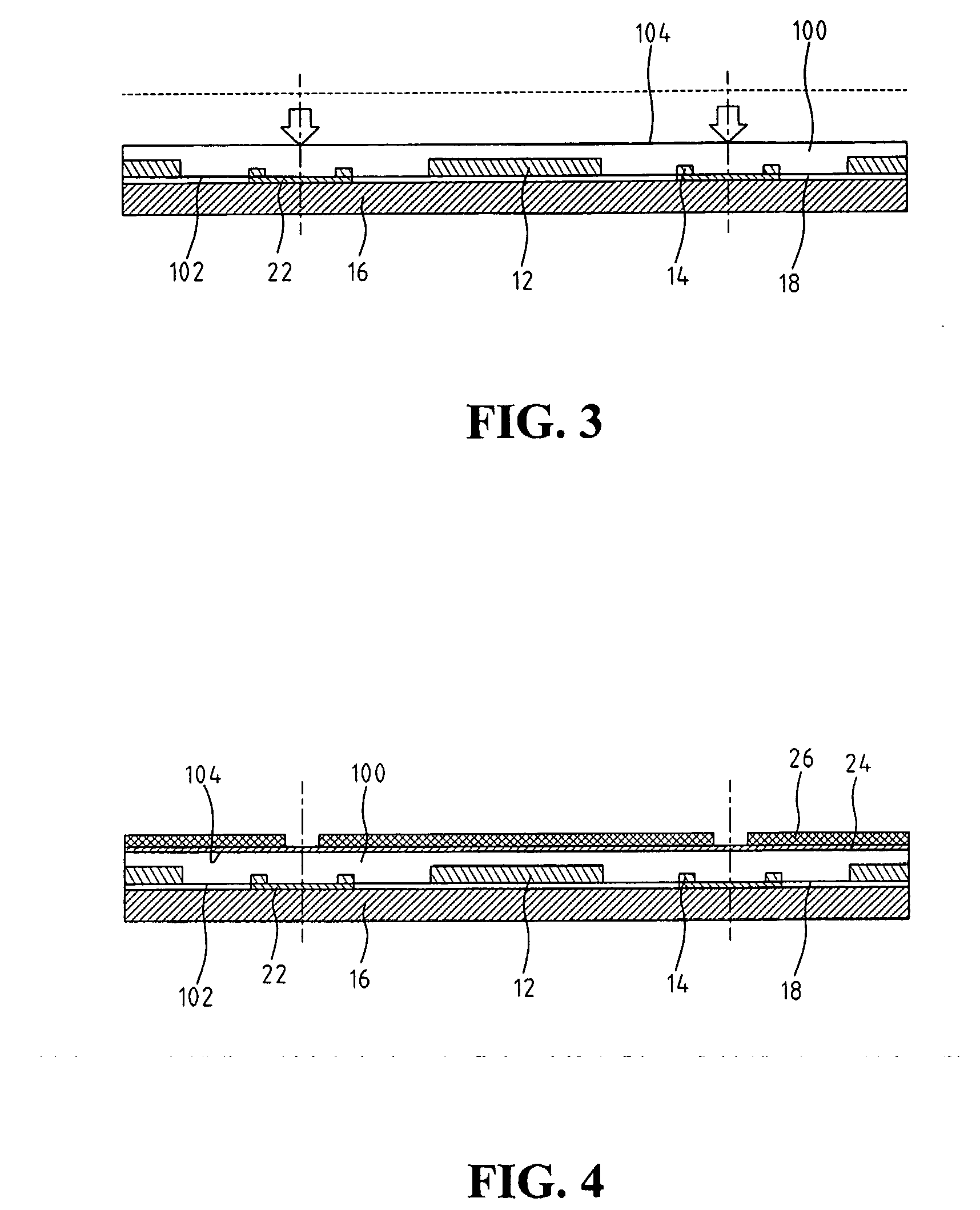
[0028] Refer to FIG. 1 and FIG. 2. The present invention discloses a wafer level package (WLP) method of sensor chip. First, a first surface 102 of a wafer 100 including a plurality of die regions 10 is bound to a transparent protective layer 16 with a glue 18. Each die region 10 of first surface 102 of wafer 100 includes an active area 12 and a pad 14 surrounding active area 12. Pad 14 is for electrical connection so that active area 12 can be electrically connected to the outside of die region 10 through pad 14. First surface 102 of wafer 100 refers to the side of wafer 100, which includes active areas 12. Transparent protective layer can be made of glass, crystal, sapphire or other conventional materials suitable for insulator allows for radiation penetration, but it is preferably to use glass. When used as spectrum filter, transparent protective layer 16 can be colored or dyed. On the other hand, at least one surface of transparent protective layer 16 is bound to a dichroic, a l...


PUM


Abstract

A method for wafer level package (WLP) of sensor chips is provided, including the steps of: providing a wafer, the wafer including a plurality of die regions, each the die region on a first surface of the wafer comprising an active area and a pad surrounding the active area; bounding a transparent protective layer to the first surface of the wafer; forming a stress buffer on a second surface of the wafer; using etching or laser drill to form a via hole at the location between two neighboring die regions through the stress buffer and the wafer to expose the pad or a conductive line between two neighboring pads; and forming a plurality of bump electrodes on the stress buffer for electrical connection to the pads through the via holes. The method can prevent pollution of the die, improve the convenience of package, reduce the manufacture cost, increase the package reliability, and solve the stress problem caused by attaching the die directly to the PCB.

Description

BACKGROUND OF THE INVENTION [0001] 1. Field of the Invention [0002] The present invention generally relates to a method for semiconductor chip packaging, and more specifically to a method for wafer level package of sensor chip. [0003] 2. The Prior Arts [0004] When the integrated circuit (IC) is designed and fabricated, the IC must be packaged. The purposes of packaging is to connect the IC with the other electrical component as to accomplish (1) power transmission, (2) electrical signal transmission, (3) provision of heat dissipation, and (4) carrying and protecting IC. [0005] As the arrival of customized electronic products, single chip products, and portable of audiovisual products, the modern demands of thin, light, short, small, new speedy, inexpensive, and environmental friendly products has driven the packaging technology going through a rapid change. At present, the chip scale package (CSP) is widely adopted. [0006] Conventional IC packaging is to dice the wafer, and the die ...

Claims


Application Information

Patent Timeline
Patent Type & Authority Applications(United States)
IPC IPC(8): H01L21/00
CPCH01L23/3114H01L27/14618H01L2924/0002H01L2924/00
Inventor WU, ENBOAYANG, ROU-CHING
Owner NAT TAIWAN UNIV
Why Eureka
Try Eureka