Method and apparatus for processing polysilazane film

a polysilazane film and processing method technology, applied in the direction of coatings, semiconductor devices, chemical vapor deposition coatings, etc., can solve the problems of difficult use as device isolation film or inter-level insulating film, poor step coverage of film, brittle film, etc., to achieve good step coverage, good film quality, and high density

Active Publication Date: 2007-10-04
TOKYO ELECTRON LTD
View PDF5 Cites 24 Cited by
  • Summary
  • Abstract
  • Description
  • Claims
  • Application Information

AI Technical Summary

Benefits of technology

[0009] An object of the present invention is to provide a method and apparatus for processing a polysilazane film, so that the polysilazane film becomes good in step coverage for a recess and high in density, and thus has good film qualities, such as electric properties and dielectric constant, used for an insulating film.

Problems solved by technology

Where a method, such as BPSG method, ozone TEOS method, or HDP method, as described above, is used to form an SiO2 film to fill a recess having a high aspect ratio, a problem arises such that the SiO2 film is very poor in filling the recess (step coverage).
However, in practice, where this method is used to form a polysilazane film, the film is brittle and therefore difficult to use as a device isolation film or inter-level insulating film.

Method used


Image

  • Method and apparatus for processing polysilazane film
  • Method and apparatus for processing polysilazane film
  • Method and apparatus for processing polysilazane film

Examples


experimental examples

[0082] Next, an explanation will be given of experimental examples performed to examine some effects of the present invention.

examples 1

Present Examples 1

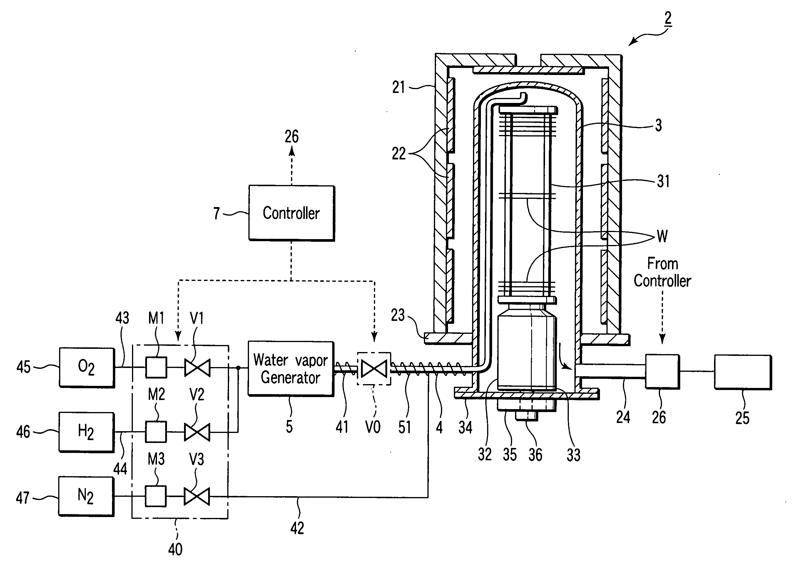
[0083] Wafers W were prepared such that a polysilazane coating film was applied to each of them and baked at 150° C. for 3 minutes. Then, the wafers W were loaded into the heat processing apparatus described above and subjected to a baking process to obtain a polysilazane film. Then, an electrical characteristic (Vfb: flat band voltage) of the polysilazane film was measured by a non-contact CV measuring unit “Quantox (product name)”. In this experiment, various heat process conditions were used for present examples in processing the polysilazane film, as follows.

[0084] Present example (PE)1-1: Only the first heat process was applied for 30 minutes, at 400° C. and normal pressure (101080 Pa), within a water vapor atmosphere (moisture concentration 80%). This result is indicated with “⋄” in FIG. 6.

[0085] Present example (PE)1-2: Only the second heat process was applied for 30 minutes, at 700° C. and normal pressure, within a water vapor atmosphere the same as that ...

examples 2

Present Examples 2

[0096] Wafers W were prepared such that a polysilazane coating film was applied to each of them and baked at 150° C. for 3 minutes. Then, the wafers W were loaded into the heat processing apparatus described above and subjected to a baking process to obtain a polysilazane film. Then, an aluminum / copper electrode pattern was formed on the polysilazane film to obtain a sample, which was used to measure the dielectric constant of the polysilazane film by a CV method. In this experiment, various heat process conditions were used for present examples in processing the polysilazane film, as follows.

[0097] Present example (PE)2-1: Only the first heat process was applied for 30 minutes, at 400° C. and normal pressure (101080 Pa), within a water vapor atmosphere (moisture concentration 80%).

[0098] Present example (PE)2-2: Only the second heat process was applied for 30 minutes, at 700° C. and normal pressure, within a water vapor atmosphere the same as that of PE2-1.

[009...


PUM

PropertyMeasurementUnit
temperatureaaaaaaaaaa

Abstract

A method of processing a polysilazane film includes a first heat process and a subsequent second heat process performed on a target substrate with a polysilazane coating film formed thereon. The first heat process is performed by supplying water vapor into a process area within a reaction container, which accommodates the target substrate, while setting the process area at a first temperature of from 390° C. to 410° C. The second heat process is performed by supplying water vapor into the process area, while setting the process area at a second temperature of from 600° C. to 800° C.

Description

CROSS-REFERENCE TO RELATED APPLICATIONS [0001] This application is based upon and claims the benefit of priority from prior Japanese Patent Application No. 2003-347420, filed Oct. 6, 2003, the entire contents of which are incorporated herein by reference. BACKGROUND OF THE INVENTION [0002] 1. Field of the Invention [0003] The present invention relates to a method and apparatus for processing a polysilazane film disposed on a target substrate, such as a silicon wafer. [0004] 2. Description of the Related Art [0005] In general, a silicon oxide film (SiO2 film) is used as an insulating film, such as a device isolation film or inter-level insulating film, for semiconductor devices. As methods of forming a silicon oxide film of this kind, a BPSG (Boron Phospho-Silicate Glass) method, ozone TEOS (TetraEthyl Ortho-Silicate) method, USG (Undoped Silicate Glass) method, and HDP (High Density Plasma enhanced chemical vapor deposition) method are known. [0006] In recent years, semiconductor de...

Claims


Application Information

Patent Timeline
Patent Type & Authority Applications(United States)
IPC IPC(8): C23C16/00B05C11/00H01L21/768H01L21/31H01L21/312H01L21/324
CPCH01L21/02164H01L21/02222H01L21/02282H01L29/78H01L21/02337H01L21/3125H01L21/76837H01L21/02318H01L21/324
Inventor HISHIYA, SHINGOAOKI, KIMIYAWATANABE, MASAHISA
Owner TOKYO ELECTRON LTD
Why Eureka
Try Eureka