

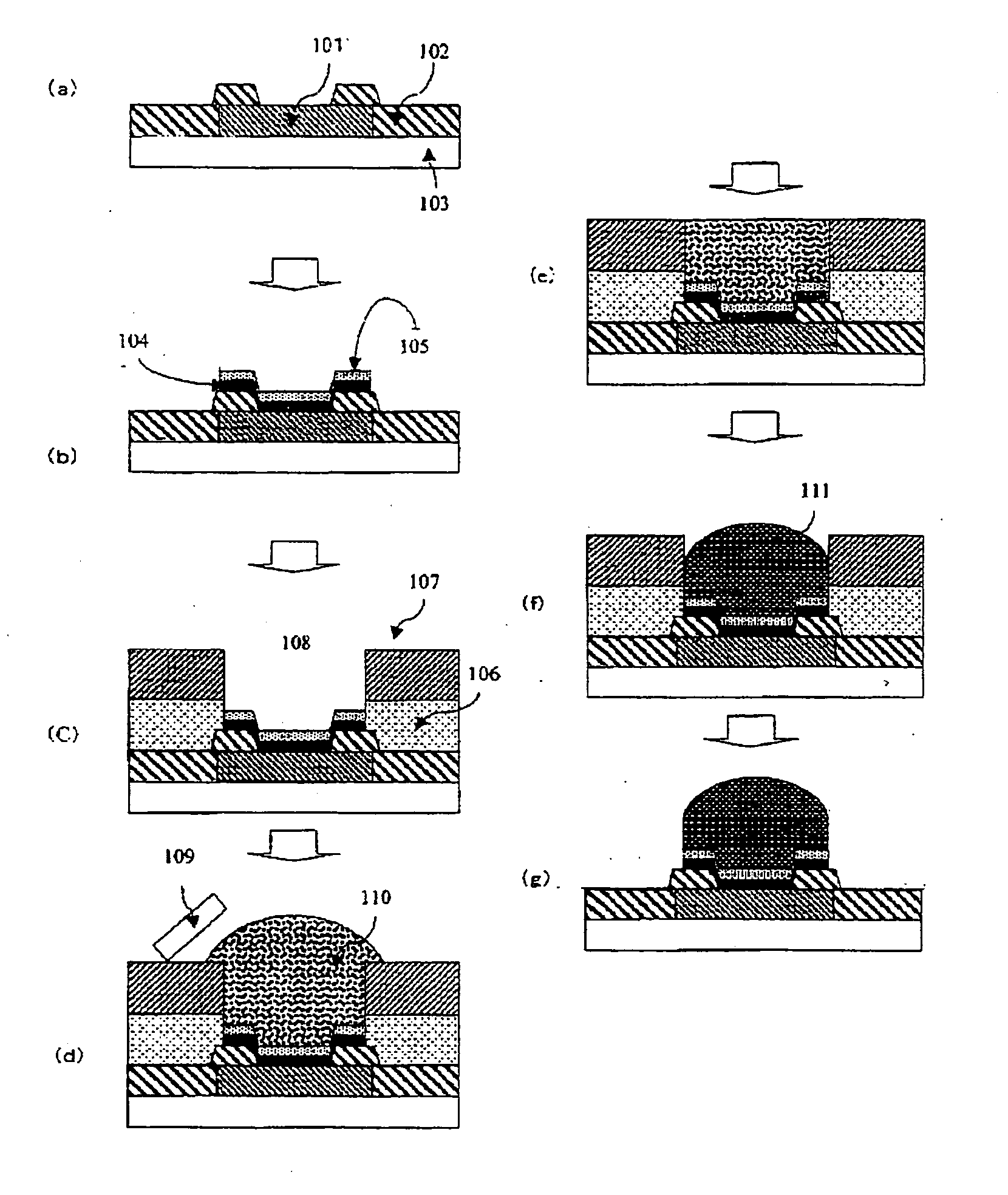
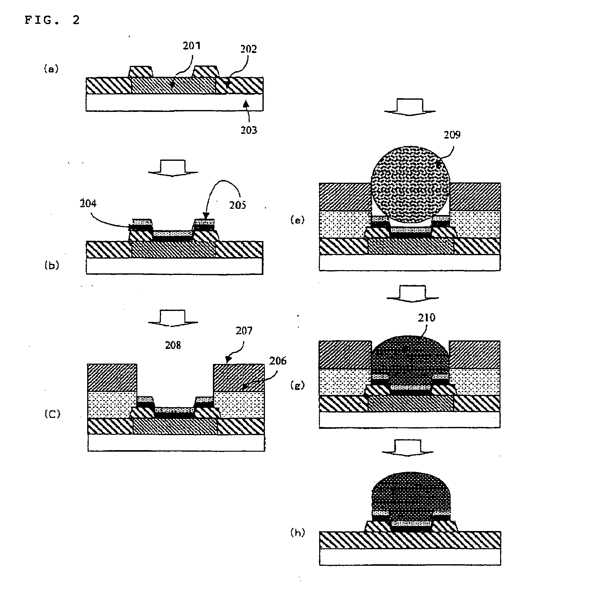
Bilayer Laminated Film for Bump Formation and Method of Bump Formation
a laminated film and bump technology, applied in the direction of resistor manufacturing, liquid/solution decomposition chemical coating, printed circuit assembling, etc., can solve the problems of difficult peeling of resists from substrates, non-uniform bump sizes, and general difficulty in peeling, etc., to achieve easy peeling and removal, good configuration, and excellent printing of solder paste
- Summary
- Abstract
- Description
- Claims
- Application Information
AI Technical Summary
Benefits of technology
Problems solved by technology
Method used
Image

Examples
synthetic example 1
Synthesis of Polymer A-1
[0222] A flask equipped with a dry ice / methanol reflux condenser and a thermometer was purged with nitrogen. The flask was charged with 100 g of N-(3,5-dimethyl-4-hydroxybenzyl)acrylamide and 300 g of methanol, followed by stirring. Subsequently, 4 g of AIBN was added, and polymerization was performed in refluxing methanol (64.5° C.) with stirring for 8 hours. After the completion of the polymerization, the polymerization solution was cooled to room temperature and was poured into a large amount of water to precipitate the polymer. The polymer was redissolved in tetrahydrofuran and was reprecipitated in a large amount of hexane. These operations were repeated three times. The precipitated product was vacuum dried at 40° C. for 48 hours to give a polymer A-1.
synthetic example 2
Synthesis of Polymer A-2
[0223] A polymer A-2 was obtained by the same procedures as the polymer A-1 was synthesized, except that 100 g of N-(3,5-dimethyl-4-hydroxybenzyl)acrylamide was replaced by 90 g of N-(3,5-dimethyl-4-hydroxybenzyl)acrylamide and 10 g of styrene.
synthetic example 3
Synthesis of Polymer A-3
[0224] A polymer A-3 was obtained by the same procedures as the polymer A-1 was synthesized, except that 100 g of N-(3,5-dimethyl-4-hydroxybenzyl)acrylamide was replaced by 65 g of N-(3,5-dimethyl-4-hydroxybenzyl)acrylamide, 15 g of styrene and 20 g of 2-hydroxyethyl acrylate.
[0225] The following compounds were used as organic solvents (B):
[0226] B-1: Ethyl 2-hydroxypropionate
[0227] B-2: Propylene glycol monomethyl ether acetate
[0228] B-3: 2-Heptanone
[0229] The following resins were used as additive resins:
[0230] Additive resin 1: Polyhydroxystyrene (Mw: 3,000)
[0231] Additive resin 2: Hydroxystyrene / styrene copolymer (feeding weight ratio: 80 / 20, Mw: 1,200)
[0232] Additive resin 3: Formalin condensate of m-cresol and p-cresol (feeding weight ratio: 60 / 40, Mw: 1,200)
[0233] Additive resin 4: 4,4′-[1-[4[1-(4-Hydroxyphenyl)-1-methylethyl]phenyl]ethylidene]diphenol
[0234] Components of upper layer compositions were as follows.
PUM
| Property | Measurement | Unit |
|---|---|---|
| Glass transition temperature | aaaaa | aaaaa |
| Fraction | aaaaa | aaaaa |
| Fraction | aaaaa | aaaaa |
Abstract
Description
Claims
Application Information