Microfluidic Device with Minimized Ohmic Resistance

a microfluidic device and ohmic resistance technology, applied in the field of miniaturisation of analytical devices, can solve the problems of unfavorable conduction current conduction of microstructures in the typical dimensions of microstructures, and achieve the effects of minimizing resistance, increasing measured signals, and improving analytical sensitivity of devices

Inactive Publication Date: 2007-10-18
DIAGNOSWISS +1
View PDF10 Cites 112 Cited by
  • Summary
  • Abstract
  • Description
  • Claims
  • Application Information

AI Technical Summary

Benefits of technology

[0024] In another embodiment, the device of the present invention constitutes a three-electrode system comprising at least one working electrode (or array of working electrodes), at least one reference electrode and at least one electrically conductive means. In one embodiment, the electrically conductive means can be adapted to directly serve as counter electrode. In another embodiment, the electrically conductive means is not part of the three-electrode system, it is not connected to the electrodes, and the device further comprises at least one additional electrode serving as counter-electrode.
[0025] In an embodiment, the microfluidic device of the invention comprises an electrically conductive means along the entire length of the microstructure, and the electrically conductive means can advantageously surround the microstructure and form a frieze of conducting material in contact with the solution present in the microstructure.
[0026] In a further embodiment, the electrically conductive means and the reference or pseudo-reference electrode can also be short-circuited. This can for instance be achieved by providing a microfluidic device where the electrically conductive means is a conducting pad forming a frieze around the microstructure which encompasses the inlet and / or outlet and where the reference or pseudo-reference electrode is simply deposited on this conducting pad on the external side of the inlet and / or outlet but a such a manner that is is in contact with the solution.
[0027] In some applications of the present invention, the counter-electrode can be used to re-generate the product of the reaction taking place at the working electrode(s), thereby increasing the measured signal and hence improving the analytical sensitivity of the device. The electrically conductive means can advantageously be used for this purpose; in such a case, the electrically conductive means would play both the roles of counter-electrode, of re-generation of the compound to detect and of minimizing the resistance along the microstructure.
[0028] In a further embodiment of the present invention, the microfluidic device may comprise at least one biological and / or chemical entity. Such a biological or chemical moiety can be immobilized either by physisorption, covalent binding, ionic bonding or simply dried on at least one portion of at least one wall of the microstructure(s). In another embodiment, the microfluidic device may also comprise beads and / or a membrane (which can be placed for instance at the inlet and / or outlet of the microstructure) so as to capture one or a plurality of target sample molecules or to wash or desalt a sample. Such beads or membrane may also comprise one or a plurality of biological and / or chemical entity(ies), which can be immobilized on these types of supports.
[0029] The microstructure walls and / or the integrated electrode(s) or electrically conductive means can also be partially coated by an organic phase (solidified or not) that can for instance be used as a protective layer for the electrode(s) or as a phase immiscible with the sample solution and can be set-up for measurements of ion transfer reactions at the interface between two immiscible solutions and can for instance be used for the dosage of ions.

Problems solved by technology

One of the constraints of microfluidic systems is that the typical dimensions of the microstructures are quite unfavourable against the conduction of current.

Method used


Image

  • Microfluidic Device with Minimized Ohmic Resistance
  • Microfluidic Device with Minimized Ohmic Resistance
  • Microfluidic Device with Minimized Ohmic Resistance

Examples


Embodiment Construction

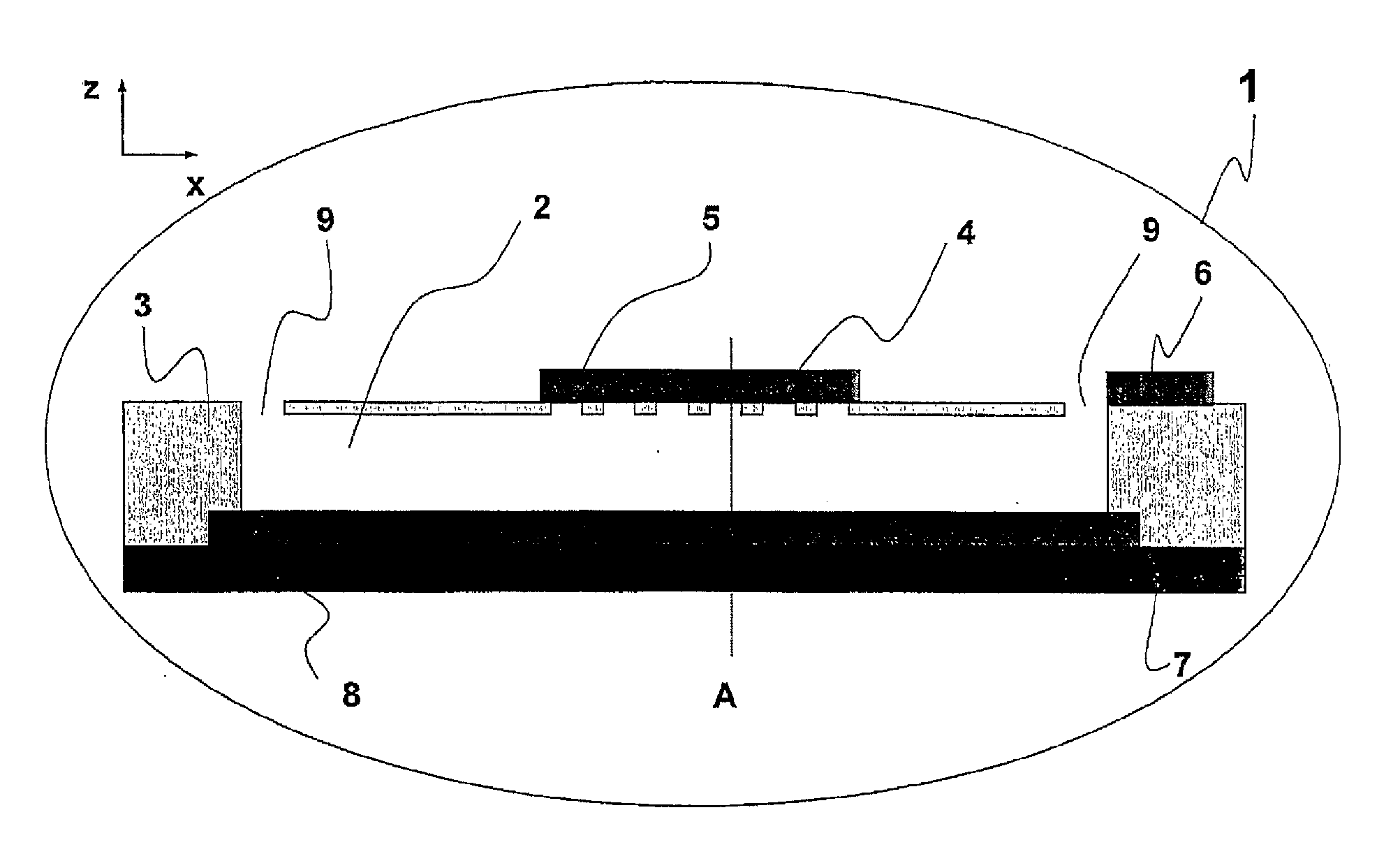
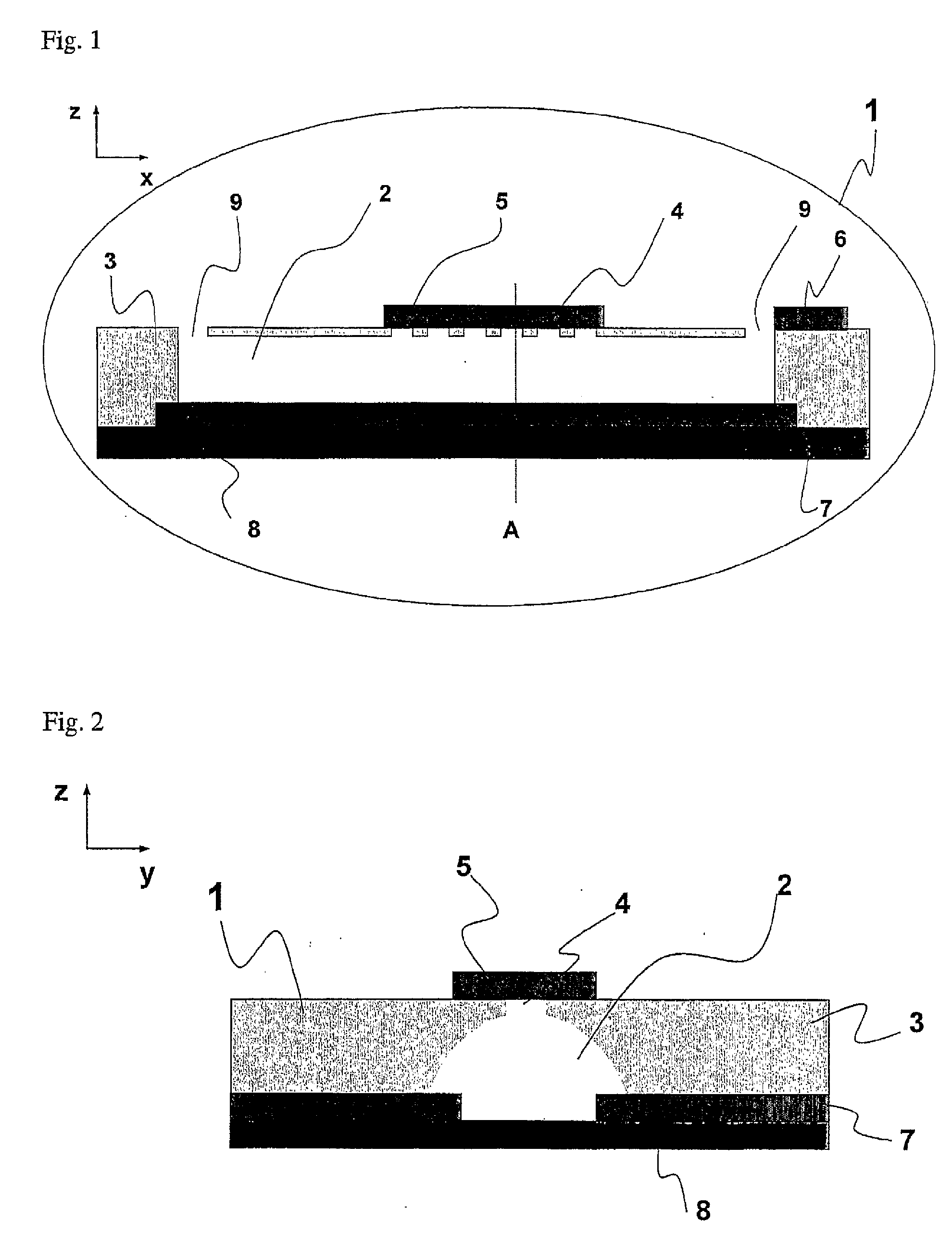
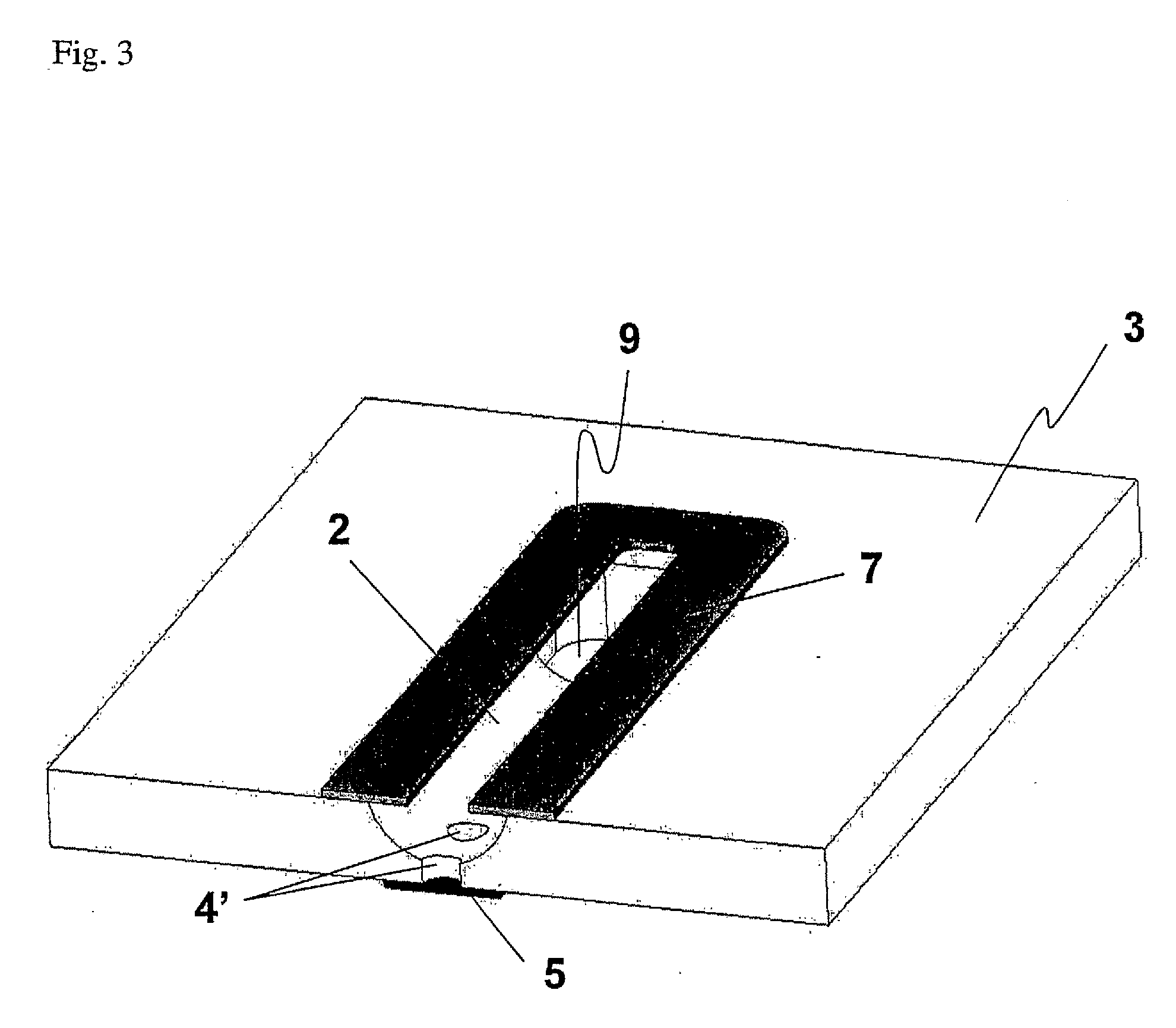
[0053]FIG. 1 is a longitudinal cross-section view of an example of microfluidic device of the present invention (1) which comprises a microstructure (2) fabricated in a substrate (3) (selected preferentially from, but not limited to, a non-conducting polymer material), said microstructure comprising one or a plurality of microelectrode(s) or microelectrode array(s) (4) as working electrode(s), generally exhibiting one or several conducting connection pad(s) (5) for connection to an external potentiostat, as well as an electrically conductive means (7) which is in direct contact with the microstructure(s) and which, in the present case, is placed in front of the working microelectrode(s), on the opposite side of the microstructure substrate. The microstructure of FIG. 1 is sealed by a cover layer (8), which can for instance be glued or laminated at the end of the fabrication process. In the case of FIG. 1, the microstructure is a microchannel comprising access holes (9) serving as in...


PUM

PropertyMeasurementUnit
capillary radiusaaaaaaaaaa
resistanceaaaaaaaaaa
thicknessaaaaaaaaaa

Abstract

An electrochemical microfluidic device has one or a plurality of microstructures, such as a microchannel, in which an electrically conductive means is integrated to reduce the ohmic resistance within the microstructure and hence to improve electrochemical measurements particularly when large current densities are involved. The electrically conductive means can be connected as a counter-electrode and can be used to re-generate the product of the reaction occurring at the working electrode. A method of fabricating electrochemical microfluidic devices comprising such an electrically conductive means is also disclosed. The invention may particularly be used in all electrochemical sensor applications where detection is performed in small volumes.

Description

BACKGROUND TO THE INVENTION [0001] Miniaturisation of analytical devices has become a trend in analytical chemistry for two main reasons: reducing the time required for single analyses and reducing the size of the sample / waste. Many developments have been shown over the last years in the fabrication of microfluidic device and their use for developing assays. [0002] One bottleneck of miniaturisation of analytical systems is to ensure a low limit of detection of the low number of molecules present in the small volume of the microfluidic device. Different detection means including optical, mass spectrometry or electrochemical detection have been implemented with success to detect rather large concentrations of analyte. For example, many microsystems exist for the detection of glucose in microfluidic devices, for example the system developed by Therasense and which allows one to perform a coulometric detection in only 0.3 μL of capillary blood. Detecting low concentrations while ensurin...

Claims


Application Information

Patent Timeline
Patent Type & Authority Applications(United States)
IPC IPC(8): G01N27/26B23P15/00
CPCB01L3/5027B01L3/502707B01L2300/0645Y10T29/53204B01L2400/0406C12Q1/001G01N33/5438B01L2300/0825
Inventor REYMOND, FREDERICROSSIER, JOEL STEPHANEMORIER, PATRICK
Owner DIAGNOSWISS
Why Eureka
Try Eureka