Method for reducing topography of non-volatile memory and resulting memory cells

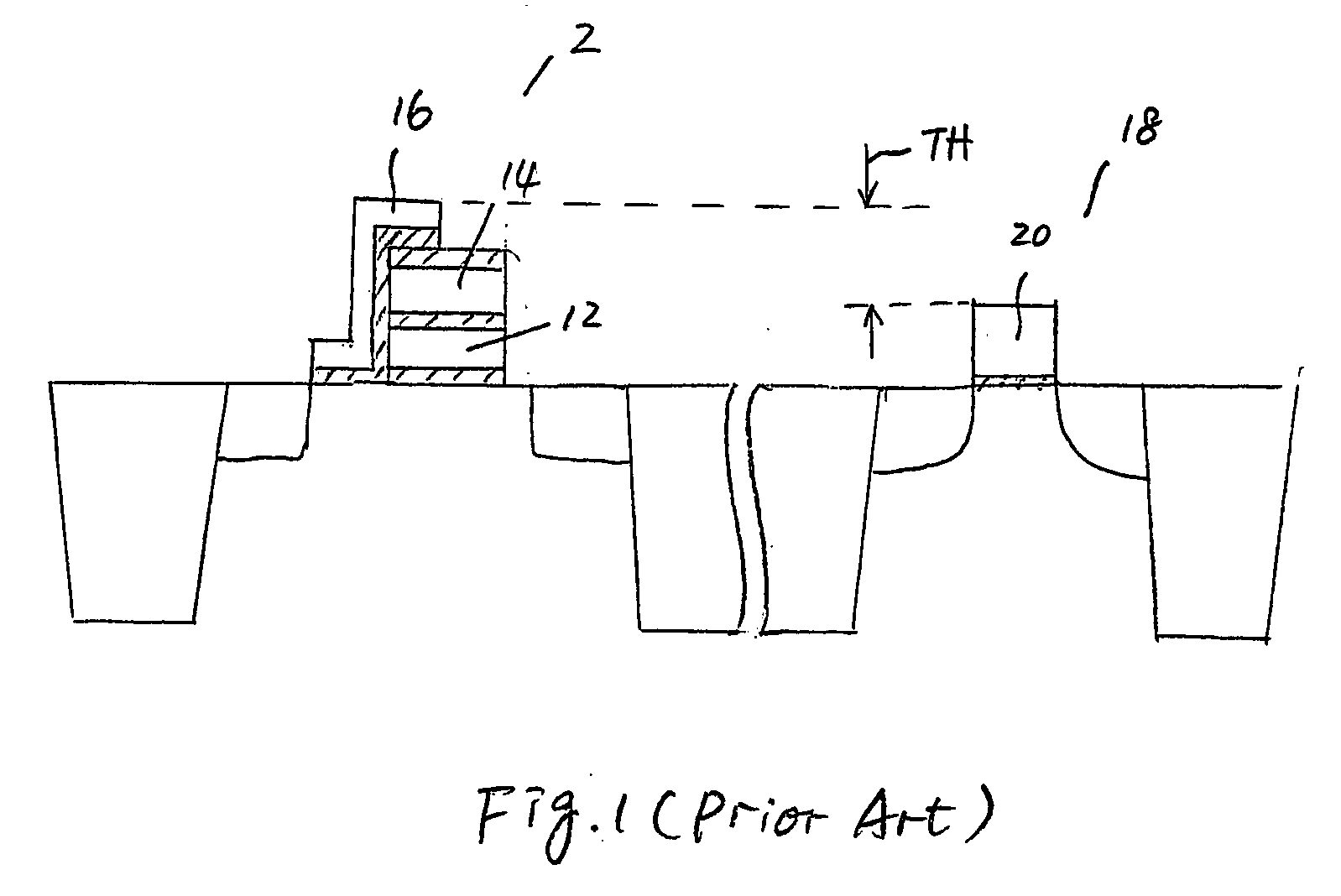
a topography and non-volatile memory technology, applied in the direction of semiconductor devices, basic electric elements, electrical appliances, etc., can solve the problems of difficult to overcome the height difference between the topography and the mos device on the same chip, the lithography instrument is difficult to measure and align to the surface of the wafer, and the photo resist is underexposure, etc., to achieve the effect of reducing the thickness of the portion, reducing the height difference, and reducing the topography height difference between the flash memory

Active Publication Date: 2007-10-18
TAIWAN SEMICON MFG CO LTD
View PDF9 Cites 56 Cited by
  • Summary
  • Abstract
  • Description
  • Claims
  • Application Information

AI Technical Summary

Benefits of technology

[0011]In accordance with yet another aspect of the present invention, a method for forming a semiconductor structure includes providing a substrate; forming a gate stack of a flash memory cell, wherein a top portion of the gate stack comprises a capping layer; forming a gate having at least a portion over the capping layer; and reducing a thickness of the portion of the gate over the capping layer.
[0012]In accordance with yet another aspect of the present invention, a method for forming a semiconductor structure includes providing a substrate comprising a cell region and a non-cell region; forming a first gate stack of a flas...

Problems solved by technology

For small-scale integrated circuit formation technologies, such as 90 nm and lower, the topography height difference is hard to overcome.
Therefore, any process variation may cause under-exposure ...

Method used


Image

  • Method for reducing topography of non-volatile memory and resulting memory cells
  • Method for reducing topography of non-volatile memory and resulting memory cells
  • Method for reducing topography of non-volatile memory and resulting memory cells

Examples


first embodiment

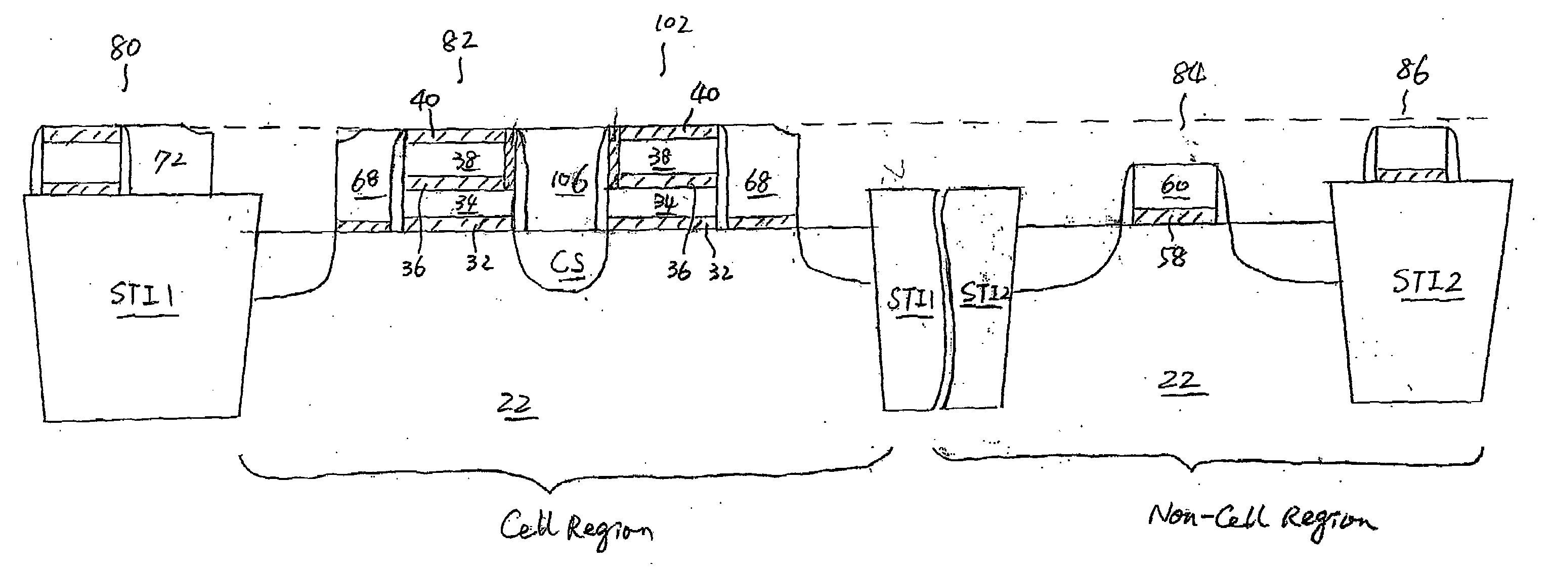
[0043]Due to the height difference SH (refer to FIG. 6) and the variation in thicknesses of the stacked layers 32, 34, 36, 38 and 40, the top surface of the capping layer 40 in the cell region may be higher or lower than the top surface 94 of the gate electrode 60 (and / or the top surface 96 of dummy feature 86). This leads to several embodiments. In the present invention, as is shown in FIG. 12, the top surface of the capping layer 40 is higher than the top surfaces 94 and 96. To reduce the height difference, a CMP is performed to recess the top surface 92 and / or the top surface 90. FIG. 13 illustrates that the top surfaces 90 and 92 are recessed (reduced) to the top surface of capping layer 40. Dummy gate 72 is also recessed simultaneously. As top surfaces 94 and 96 are lower than the top surface of capping layer 40, they are not recessed.

second embodiment

[0044]It should be appreciated that the CMP or selective dry etching back may be stopped before the top surface of capping layer 40 is reached, and thus the top surfaces 90 and 92 will be higher than as shown in FIG. 13. FIG. 14 illustrates a resulting second embodiment of the present invention.

[0045]Wordline 68 preferably includes three portions, a higher portion 68, directly over the floating gate 34, a vertical portion 682, and a lower portion 683 over the channel region. Portions 681 and 683 may have substantially flat top surfaces. Before CMP, the portions 681 and 683 of the wordline 68 and gate electrode 60 all have a substantially equal thickness TG. After CMP, the thickness TG of the gate electrode 60 will be greater than the thickness TG′ of the higher wordline portion 681. Also, the thickness TG of the portion 683 of the wordline 68 will be greater than the thickness TG′ of the portion 681 of the wordline 68. In FIG. 13, the thickness TG′ of the portion 681 is reduced to z...

third embodiment

[0046]In a third embodiment, dry etching is used to recess the top surfaces 90 and 92, as is shown in FIG. 15, wherein dashed lines indicate the original positions of features 68 and 72. The non-cell region is preferably protected during the dry etching. As a result, the thickness TG′ of the wordline 68 and dummy pattern 72 are substantially equally reduced, and is less than the thickness TG of the gate electrode 60 in the non-cell region. Preferably, after the recession of the top surfaces 90 and 92, a combined thickness, which includes thickness TG′ and the thicknesses of layers 34, 36, 38 and 40, is preferably less than about 150 percent of the thickness TG. Thicknesses TG and TG′ preferably have a difference of less than about 1000 Å.


PUM


Abstract

A method for forming a semiconductor structure includes providing a substrate; forming a gate stack of a flash memory cell, wherein a top portion of the gate stack comprises a capping layer; forming a gate having at least a portion over the capping layer; and reducing a thickness of the portion of the gate over the capping layer. The topography height difference between the flash memory cell and MOS devices on the same chip is reduced.

Description

[0001]This application claims the benefit of U.S. Provisional Application No. 60 / 791,728, filed on Apr. 13, 2006, entitled “Method for Reducing Topography of Non-Volatile Memory and Resulting Memory Cells,” which application is hereby incorporated herein by reference.TECHNICAL FIELD[0002]This invention relates generally to semiconductor devices, and more particularly to the structure and manufacturing methods of flash memory cells.BACKGROUND[0003]Flash memory has become increasingly popular in recent years. A typical flash memory comprises a memory array having a large number of memory cells arranged in blocks. Each of the memory cells is fabricated as a field-effect transistor having a control gate and a floating gate. The floating gate is capable of holding charges and is separated from source and drain regions contained in a substrate by a layer of thin oxide. Each of the memory cells can be electrically charged by injecting electrons from the drain region through the oxide layer...

Claims


Application Information

Patent Timeline
IPC IPC(8): H01L29/76
CPCH01L27/105H01L27/11521H01L27/11573H01L27/11568H01L27/11526H10B41/40H10B41/30H10B43/30H10B43/40
Inventor WANG, SHIH WEILIN, DEREKHUANG, CHEN-MINGHSIEH, CHANG-JENLO, CHI-HSINYU, CHUNG-YISHIU, FENG-JIATU, YEUR-LUENCHU, YI-SHINYANG, JEN-SHENG
Owner TAIWAN SEMICON MFG CO LTD
Why Eureka
Try Eureka