Dual plasma source process using a variable frequency capacitively coupled source to control plasma ion density

a capacitively coupled source and plasma ion technology, applied in the direction of instruments, fluid pressure measurement, coatings, etc., can solve the problems of not all process parameters can be independently controlled, non-uniform plasma density is introduced into the processing, and non-uniformity becomes more critical

Active Publication Date: 2007-10-25
APPLIED MATERIALS INC
View PDF99 Cites 33 Cited by
  • Summary
  • Abstract
  • Description
  • Claims
  • Application Information

AI Technical Summary

Benefits of technology

[0006] VHF plasma source power into a process region of the chamber that overlies the wafer, and (b) inductively coupling RF plasma source power into the process region, and controlling plasma ion density by controlling the effective frequency of the VHF source power. In a preferred e

Problems solved by technology

In semiconductor fabrication processes, conventional sources of plasma source power, such as inductively coupled RF power applicators or capacitively couple RF power applicators, introduce inherent plasma density non-uniformities into the processing.
As device geometries have continued to shrink, such non-uniformities become more critical, requiring better compensation.
However, a large ceiling-to-wafer distance can prevent the beneficial gas distribution effects of a ceiling gas distribution showerhead from reaching the wafer surface, due to diffusion over the large distance.
One limitation of such react

Method used


Image

  • Dual plasma source process using a variable frequency capacitively coupled source to control plasma ion density
  • Dual plasma source process using a variable frequency capacitively coupled source to control plasma ion density
  • Dual plasma source process using a variable frequency capacitively coupled source to control plasma ion density

Examples


first embodiment

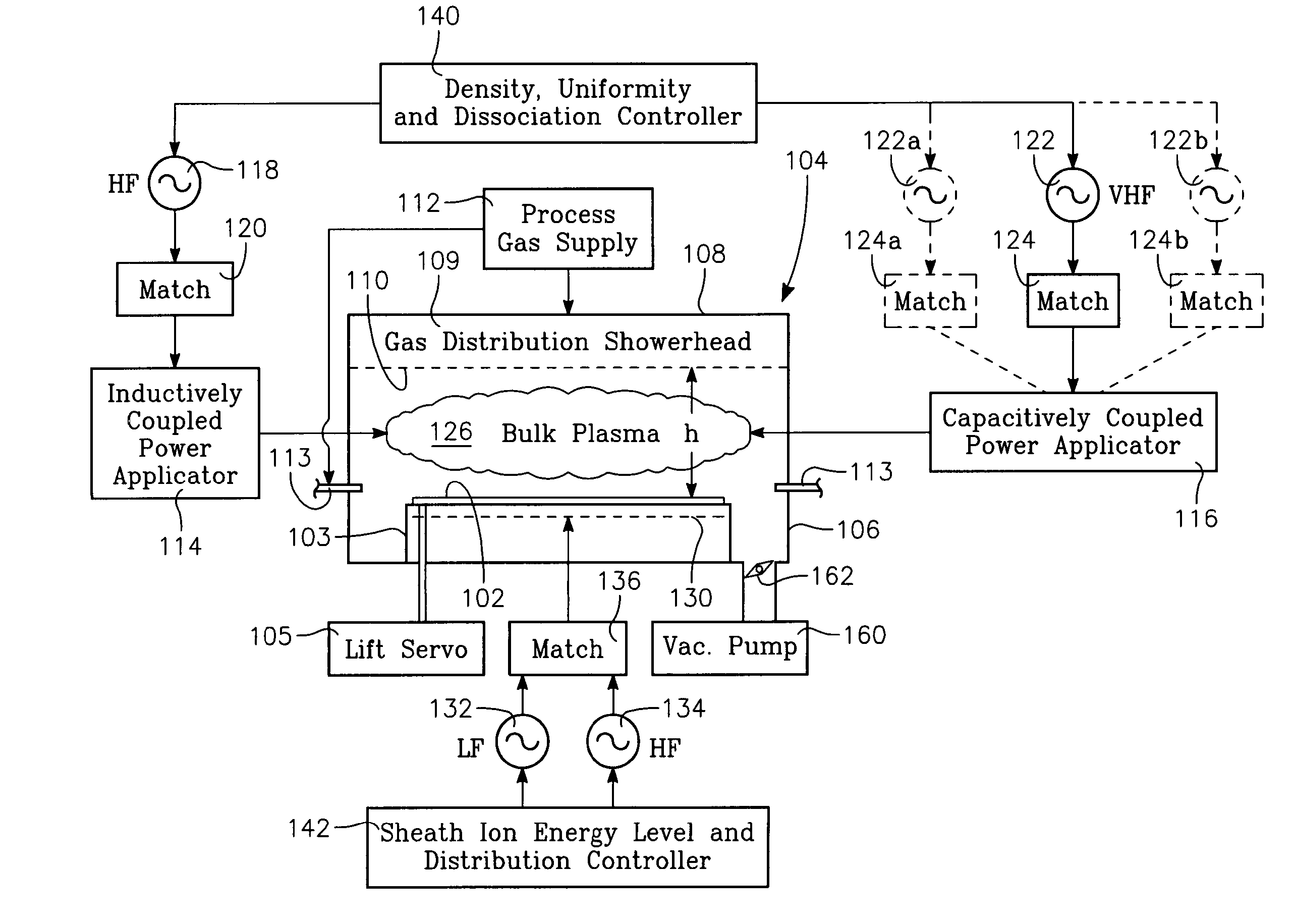
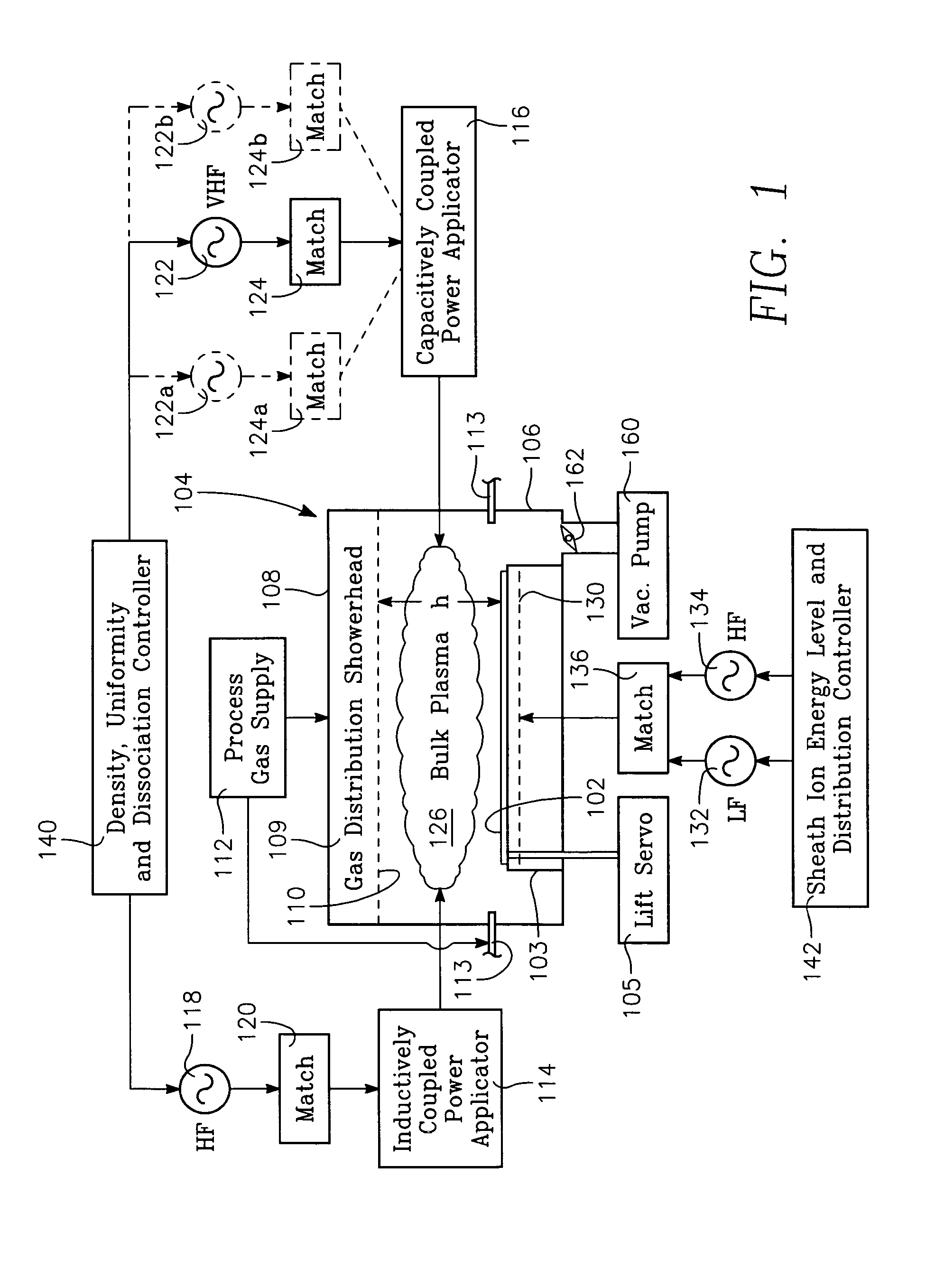
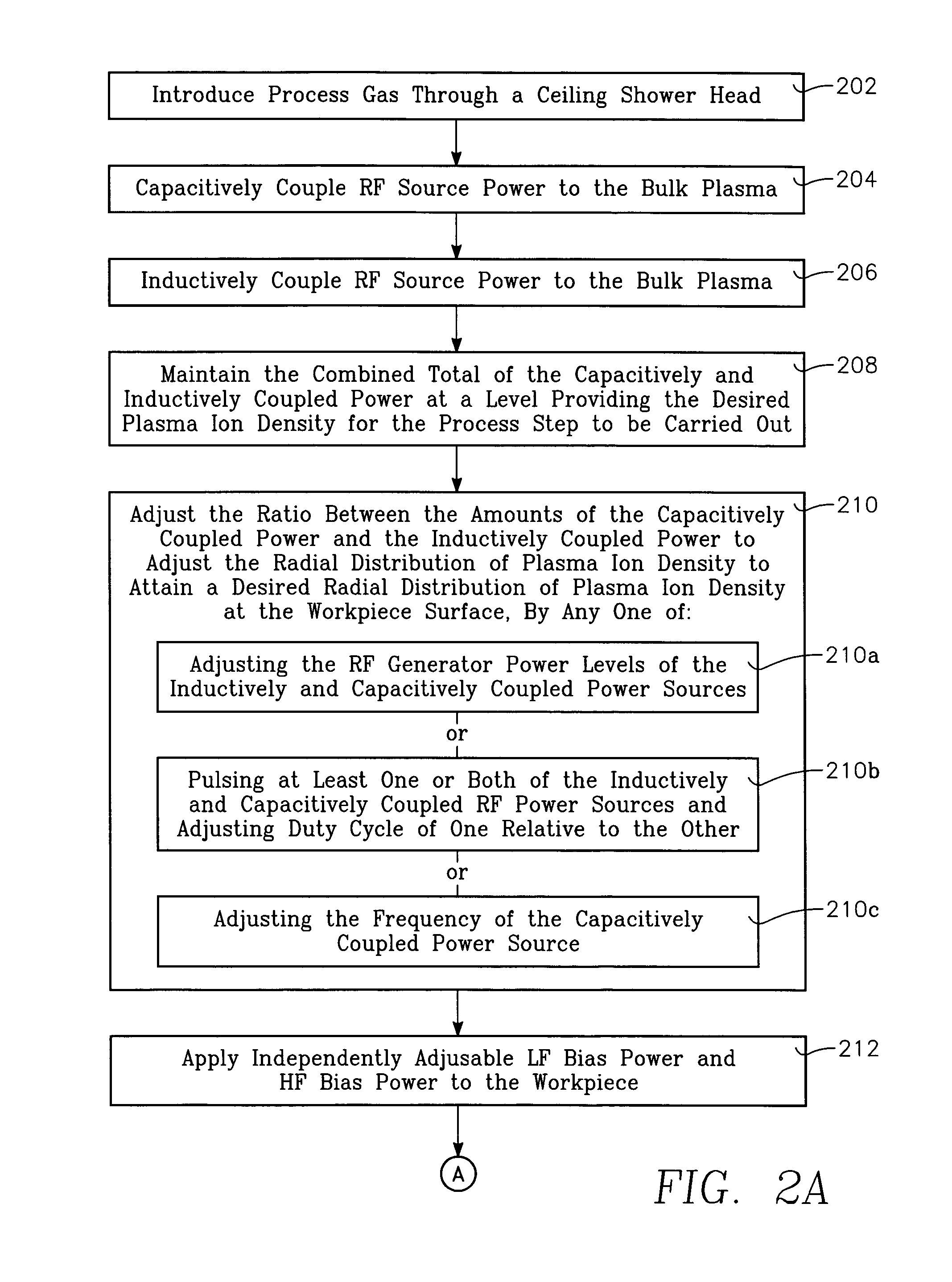
[0072]FIG. 19 illustrates a plasma reactor of the invention for processing a workpiece 102, which may be a semiconductor wafer, held on a workpiece support 103 within a reactor chamber 104. Optionally, the workpiece support 103 be raised and lowered by a lift servo 105. The chamber 104 is bounded by a chamber sidewall 106 and a ceiling 108. The ceiling 108 may include a gas distribution showerhead 109 having small gas injection orifices 110 in its interior surface, the showerhead 109 receiving process gas from a process gas supply 112. The reactor includes an inductively coupled RF plasma source power applicator 114. As illustrated in FIG. 22, the inductively coupled power applicator may consist of a conductive coil 114a wound in a helix and lying over the ceiling 108 in a plane parallel to the ceiling 108. Alternatively, as depicted in FIG. 23, the conductive coil may consist of parallel helically wound conductors 114b, 114c, 114d. A capacitively coupled RF plasma source power appl...

third embodiment

[0074] An RF power generator 118 provides high frequency (HF) power (e.g., within a range of about 10 MHz through 27 MHz) through an impedance match element 120 to the inductively coupled coil antenna 114a. In one embodiment in which the ceiling electrode 116a is the capacitively coupled source power applicator, an RF power generator 122 provides very high frequency (VHF) power (e.g., within a range of about 27 MHz through 200 MHz) through an impedance match element 124 to the capacitively coupled power applicator 116. In another embodiment in which the bottom (workpiece support) electrode 130 is the capacitively coupled source power applicator, an RF power generator 123 provides VHF power through an impedance match element 125 to the bottom electrode 130. In a third embodiment, both the ceiling and bottom electrodes 116a, 130 comprise the capacitively coupled plasma source power applicator, so that both VHF generators 122, 123 are present. In a further embodiment, both electrodes 1...


PUM

PropertyMeasurementUnit
Timeaaaaaaaaaa
Densityaaaaaaaaaa
Ratioaaaaaaaaaa

Abstract

A method of processing a workpiece in the chamber of a plasma reactor includes introducing a process gas into the chamber, simultaneously (a) capacitively coupling VHF plasma source power into a process region of the chamber that overlies the wafer, and (b) inductively coupling RF plasma source power into the process region, and controlling plasma ion density by controlling the effective frequency of the VHF source power. In a preferred embodiment, the step of coupling VHF source power is performed by coupling VHF source power from different generators having different VHF frequencies, and the step of controlling the effective frequency is performed by controlling the ratio of power coupled by the different generators.

Description

BACKGROUND OF THE INVENTION [0001] In semiconductor fabrication processes, conventional sources of plasma source power, such as inductively coupled RF power applicators or capacitively couple RF power applicators, introduce inherent plasma density non-uniformities into the processing. In particular, inductively coupled plasma sources are characterized by an “M”-shaped radial distribution of plasma ion density over the semiconductor workpiece or wafer. As device geometries have continued to shrink, such non-uniformities become more critical, requiring better compensation. Presently, the non-uniformity of an overhead inductively coupled source is reduced or eliminated at the wafer surface by optimizing the coil design and ceiling-to-wafer distance, aspect ratio, of the chamber. This distance must be sufficient so that diffusion effects can overcome the effects of the nonuniform ion distribution in the ion generation region before they reach the wafer. For smaller device geometries on ...

Claims


Application Information

Patent Timeline
IPC IPC(8): C23C16/00
CPCH01J37/32091H01J37/32165H01J37/321
Inventor PATERSON, ALEXANDERTODOROW, VALENTIN N.PANAGOPOULOS, THEODOROSHATCHER, BRIAN K.KATZ, DANHAMMOND, EDWARD P. IVHOLLAND, JOHN P.MATYUSHKIN, ALEXANDER
Owner APPLIED MATERIALS INC
Why Eureka
Try Eureka